
Wire bonding method and wire bonding structure

A technology of wire bonding and metal wire, which is applied in the field of wire bonding and wire bonding structure, can solve problems such as cost increase, grain damage, and influence on interconnection structure, and achieve the effect of reducing consumption

Inactive Publication Date: 2018-03-06
NAN YA TECH
View PDF4 Cites 0 Cited by
  • Summary
  • Abstract
  • Description
  • Claims
  • Application Information

AI Technical Summary

Problems solved by technology

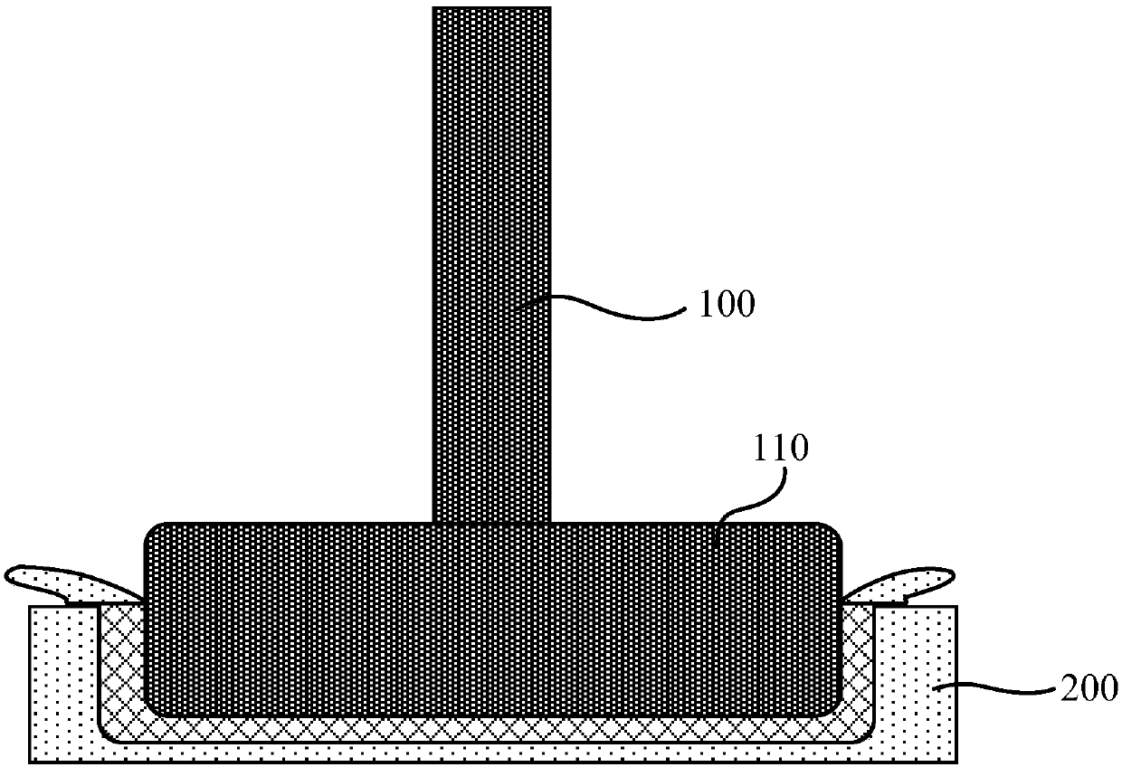
Once the thickness of the bonding pad 200 is too thin, the aforementioned step of pressing the ball bonding structure 110 and / or the step of applying ultrasonic energy may easily cause damage to the die (eg, cracks), which may further affect the interconnection structure and thus cause abnormal electrical signals
In other words, the thin bonding pad 200 cannot provide die cushioning effect
In order to solve this problem, the thickness of the bonding pad 200 can be increased, but the cost will also increase

Method used


Image

  • Wire bonding method and wire bonding structure
  • Wire bonding method and wire bonding structure
  • Wire bonding method and wire bonding structure

Examples


Embodiment Construction

[0035] A number of implementations of the present invention will be disclosed below with the accompanying drawings. For the sake of clarity, many practical details will be described together in the following description. It should be understood, however, that these practical details should not be used to limit the invention. That is, in some embodiments of the present invention, these practical details are unnecessary. In addition, for the sake of simplifying the drawings, some well-known and commonly used structures and components will be shown in a simple and schematic manner in the drawings. And, unless otherwise indicated, the same component symbols in different drawings can be considered as corresponding components. The drawing in these drawings is for clearly expressing the connection relationship among the various components in these embodiments, and does not show the actual size of each component.

[0036] Please refer to Figure 2 to Figure 4D . figure 2 It is a ...


PUM

PropertyMeasurementUnit
thicknessaaaaaaaaaa

Abstract

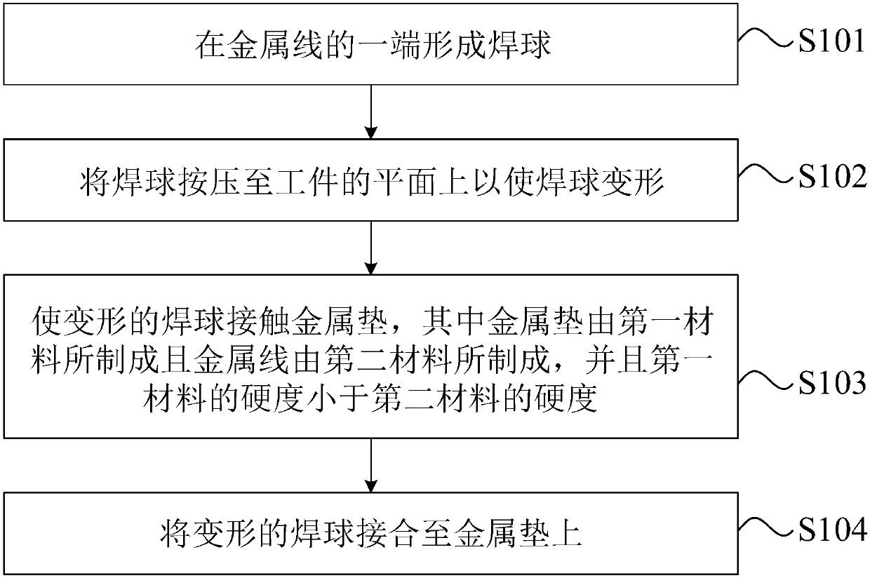
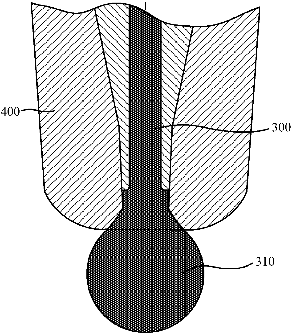
The invention discloses a wire bonding method and a wire bonding structure. The wire bonding method includes steps of: forming a Free Air Ball (FAB) at an end of a metal wire; pressing the FAB onto aflat surface of a workpiece to deform the FAB; contacting the deformed FAB to a metal pad, wherein the metal pad is made of a first material and the metal wire is made of a second material, and a hardness of the first material is smaller than a hardness of the second material; and bonding the deformed FAB on the metal pad. The wire bonding method of the disclosure can effectively reduce the consumption of the bonding pad and keep the original thickness of the bonding pad as possible, and the conventional problem that the structure under the bonding pad is damaged when the FAB is pressed onto the bonding pad with a high pressure can be prevented.

Description

technical field [0001] The invention relates to a wire bonding method and a wire bonding structure. Background technique [0002] A semiconductor die is a tiny integrated circuit formed from a semiconductor wafer. Dies are diced from the wafer and then attached to a substrate or semiconductor chip carrier. Bonding pads on the semiconductor die are electrically connected to electrical contacts (also referred to as wires or wire fingers) on the carrier via bonding wires (eg, using wire bonding equipment). Wire bonding is a solid phase process that uses a combination of heat, pressure, and ultrasonic energy to form a bond wire between a bond pad and a carrier lead. [0003] Such as figure 1 As shown, in a semiconductor device assembly of wire bonding type assembly, a ball bond structure 110 is generally used to attach the tip of the wire body 100 to the bonding pad 200 on the die. The ball bonding structure 110 is formed by applying a high voltage charge to the tip of the w...

Claims


Application Information

Patent Timeline
Patent Type & Authority Applications(China)
IPC IPC(8): H01L21/60H01L23/49
CPCH01L24/45H01L24/85H01L2224/4501H01L2224/85047H01L2224/85986H01L24/05H01L24/48H01L24/78H01L2224/04042H01L2224/05624H01L2224/05647H01L2224/45144H01L2224/45147H01L2224/48463H01L2224/48507H01L2224/48624H01L2224/48647H01L2224/48824H01L2224/48847H01L2224/78301H01L2224/85045H01L2224/85205H01L2924/00014H01L2924/01046H01L2924/01079H01L2224/43848H01L2224/45647
Inventor 林柏均
Owner NAN YA TECH
Learn More