Super junction device and manufacturing method thereof

A super-junction device and manufacturing method technology, applied in semiconductor/solid-state device manufacturing, semiconductor devices, electrical components, etc., can solve the problems of increasing device cost, increasing device specific on-resistance, etc., achieve device performance assurance, and improve softness factor effect

Inactive Publication Date: 2018-03-06
SHENZHEN SANRISE TECH CO LTD
View PDF4 Cites 7 Cited by
  • Summary
  • Abstract
  • Description
  • Claims
  • Application Information

AI Technical Summary

Problems solved by technology

Therefore, in the prior art, the softness factor can be improved by increasing the thickness of the buffer layer, but this will increase the cost of the device and also increase the specific on-resistance of the device.

Method used


Image

  • Super junction device and manufacturing method thereof
  • Super junction device and manufacturing method thereof
  • Super junction device and manufacturing method thereof

Examples


no. 1 example approach

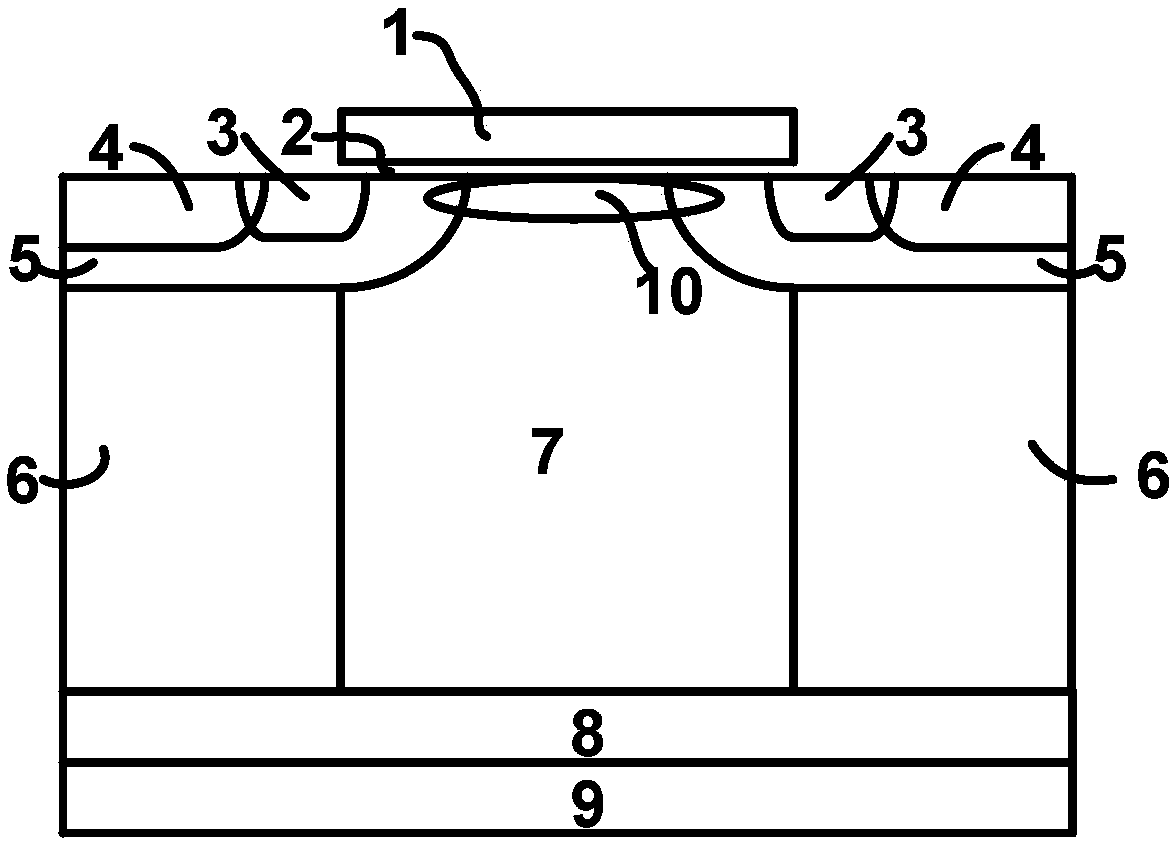
[0096] The method for manufacturing a super junction device according to the first embodiment of the present invention is used to manufacture such as image 3 The device of the first embodiment of the present invention shown, the method of the first embodiment of the present invention includes the following steps:

[0097] Step 1, such as Figure 5A As shown, an N-type epitaxial layer is provided, and the N-type epitaxial layer is formed on an N-type heavily doped semiconductor substrate 9 . The thickness of the N-type epitaxial layer includes the thicknesses of the subsequent buffer layer 8 and N-type pillars 7 . The semiconductor substrate 9 is usually a wafer structure, so it is also called a wafer.

[0098] Step two, such as Figure 5A As shown, a hard mask layer 12 is formed on the surface of the N-type epitaxial layer, and the hard mask layer 12 in the trench formation area is removed by photolithography, and all the hard mask layers outside the trench formation area ...

no. 2 example approach

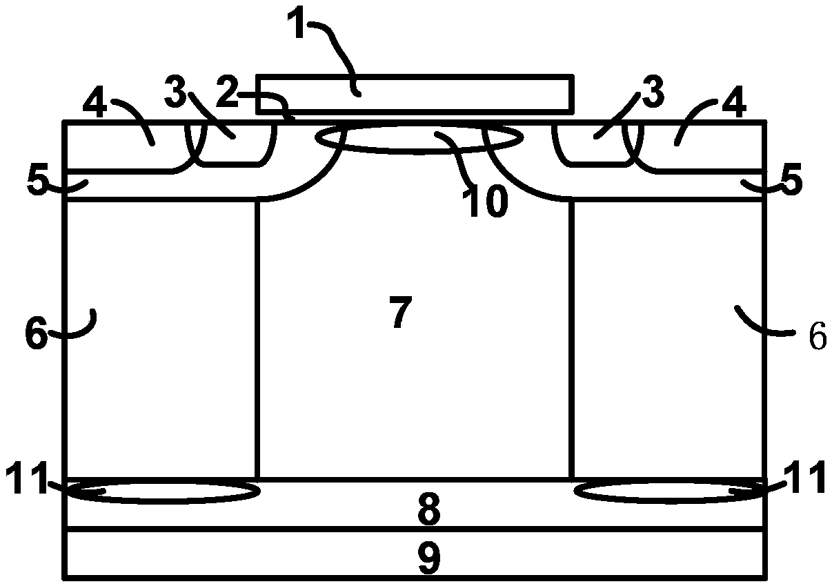
[0118] The manufacturing method of the super junction device according to the second embodiment of the present invention is used to manufacture such as Figure 4 The device of the second embodiment of the present invention shown, the method of the second embodiment of the present invention includes the following steps:

[0119] Step 1, such as Figure 6A As shown, a first epitaxial sublayer 8 with N-type doping is provided, and the first epitaxial sublayer 8 is formed on an N-type heavily doped semiconductor substrate 9 . The first epitaxial sublayer 8 is used to form a buffer layer 8 , which are all marked with 8 .

[0120] Step two, such as Figure 4 As shown, multiple epitaxy is carried out and a photolithography definition and P-type ion implantation are performed after each epitaxy process to form corresponding P-type sub-columns 13a, 13b and 13c, and the P-type sub-columns formed after each epitaxy Vertical stacking forms P-shaped columns 6 .

[0121] The epitaxial l...


PUM


Abstract

The present invention discloses a super junction device. The super junction device comprises: a super junction structure formed by first conduction type columns and second conduction type columns which are alternately arranged; channel regions; a buffer layer; a drain region formed by a semiconductor substrate at the bottom portion of the buffer layer; source regions formed at surfaces of the channel regions; one first conduction type injection region formed at the surface of the buffer layer at the bottom portion of each second conduction type column; and a parasitic body diode formed by a drift region, the channel regions and the second conduction type columns, wherein the first conduction type injection regions are configured to reduce exhaustion of the buffer layer when the parasitic body diode is reversely biased so that reversely recovered soft factors are improved. The present invention further discloses a manufacturing method of a super junction device. The reversely recoveredsoft factor can be improved, the device cost is reduced, and the specific on-state resistance of the device is reduced.

Description

technical field [0001] The invention relates to the field of manufacturing semiconductor integrated circuits, in particular to a super junction device; the invention also relates to a method for manufacturing the super junction device. Background technique [0002] The super junction structure is composed of alternately arranged N-type pillars and P-type pillars. If the superjunction structure is used to replace the N-type drift region in the vertical double-diffused MOS transistor (Vertical Double-diffused Metal-Oxide-Semiconductor, VDMOS) device, the conduction path is provided through the N-type column in the conduction state, and when the conduction The P-type column does not provide a conduction path; in the off state, the PN column jointly bears the reverse bias voltage, forming a super-junction metal-oxide-semiconductor field-effect transistor (Metal-Oxide-Semiconductor Field-Effect Transistor, MOSFET). Such as figure 1 Shown is a structural diagram of an existing s...

Claims


Application Information

Patent Timeline
Patent Type & Authority Applications(China)
IPC IPC(8): H01L29/78H01L29/06H01L21/336
CPCH01L29/0634H01L29/66712H01L29/7802H01L29/7804
Inventor 曾大杰
Owner SHENZHEN SANRISE TECH CO LTD
Why Eureka
Try Eureka