Control circuit of switching power supply device and switching power supply device
A technology for control circuits and switching power supplies, applied in electronic switches, control/regulation systems, output power conversion devices, etc., can solve the problems of MOSFET threshold voltage and gate drive voltage increase, unable to suppress back electromotive force, etc., to achieve low noise , the effect of high reliability
- Summary
- Abstract
- Description
- Claims
- Application Information
AI Technical Summary
Problems solved by technology
Method used
Image
Examples
no. 1 example
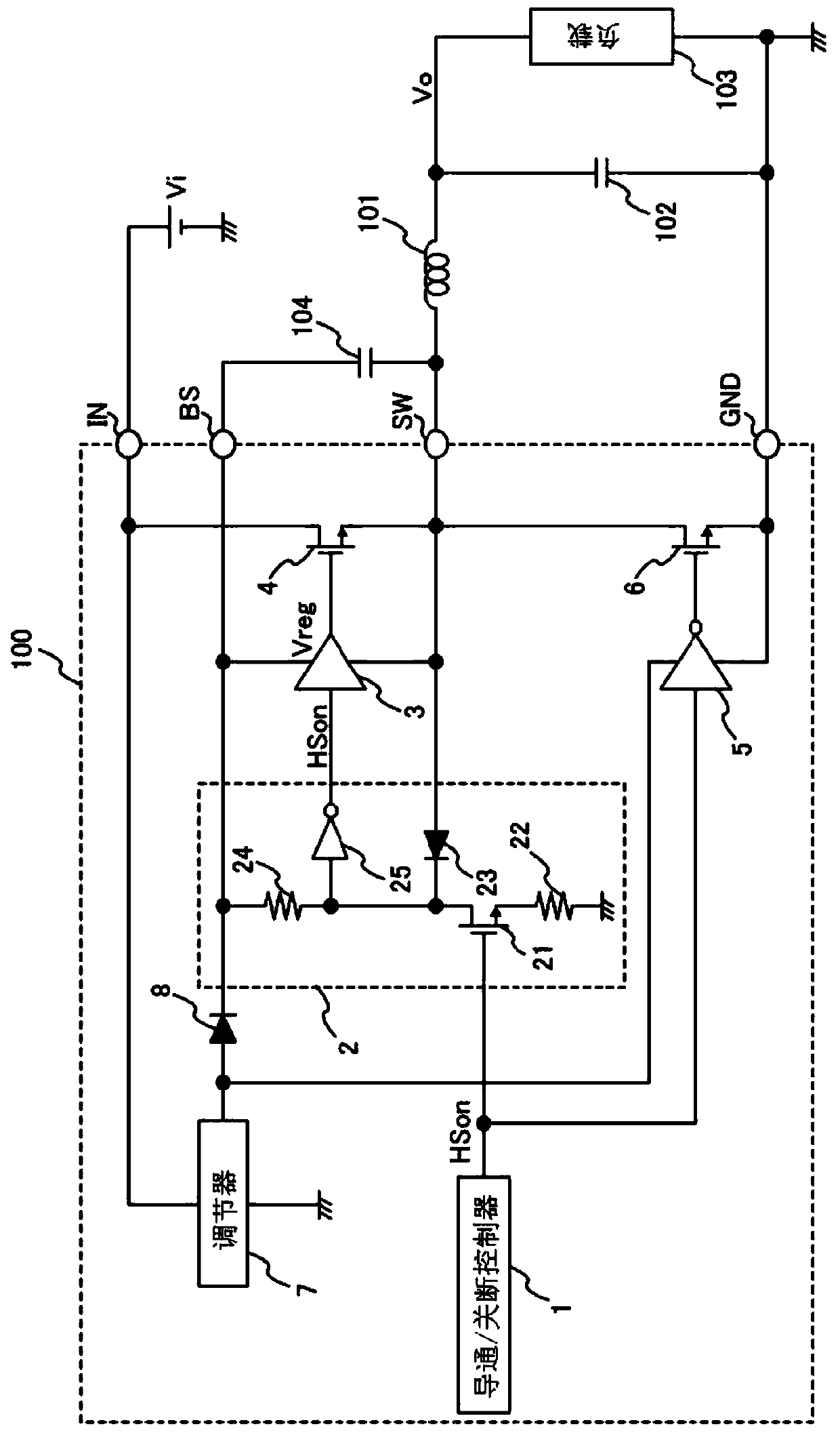
[0025] figure 1 is a circuit diagram of a switching power supply device according to an embodiment of the present invention.
[0026] figure 1 The illustrated switching power supply device includes a control circuit 100 , an inductor 101 , an output capacitor 102 , an output load 103 and a bootstrap capacitor 104 .
[0027] An input power supply supplying the first DC voltage Vi is connected to the input terminal IN of the control circuit 100 .
[0028] The inductor 101 has one end connected to the switch terminal SW of the control circuit 100 and the other end connected to the output load 103 .
[0029] The bootstrap capacitor 104 has one end connected to the bootstrap terminal BS of the control circuit 100 and the other end connected to a connection point between the switch terminal SW and the inductor 101 .
[0030] The output capacitor 102 has one end connected to the connection point between the inductor 101 and the output load 103 and the other end connected to the gr...
no. 2 example
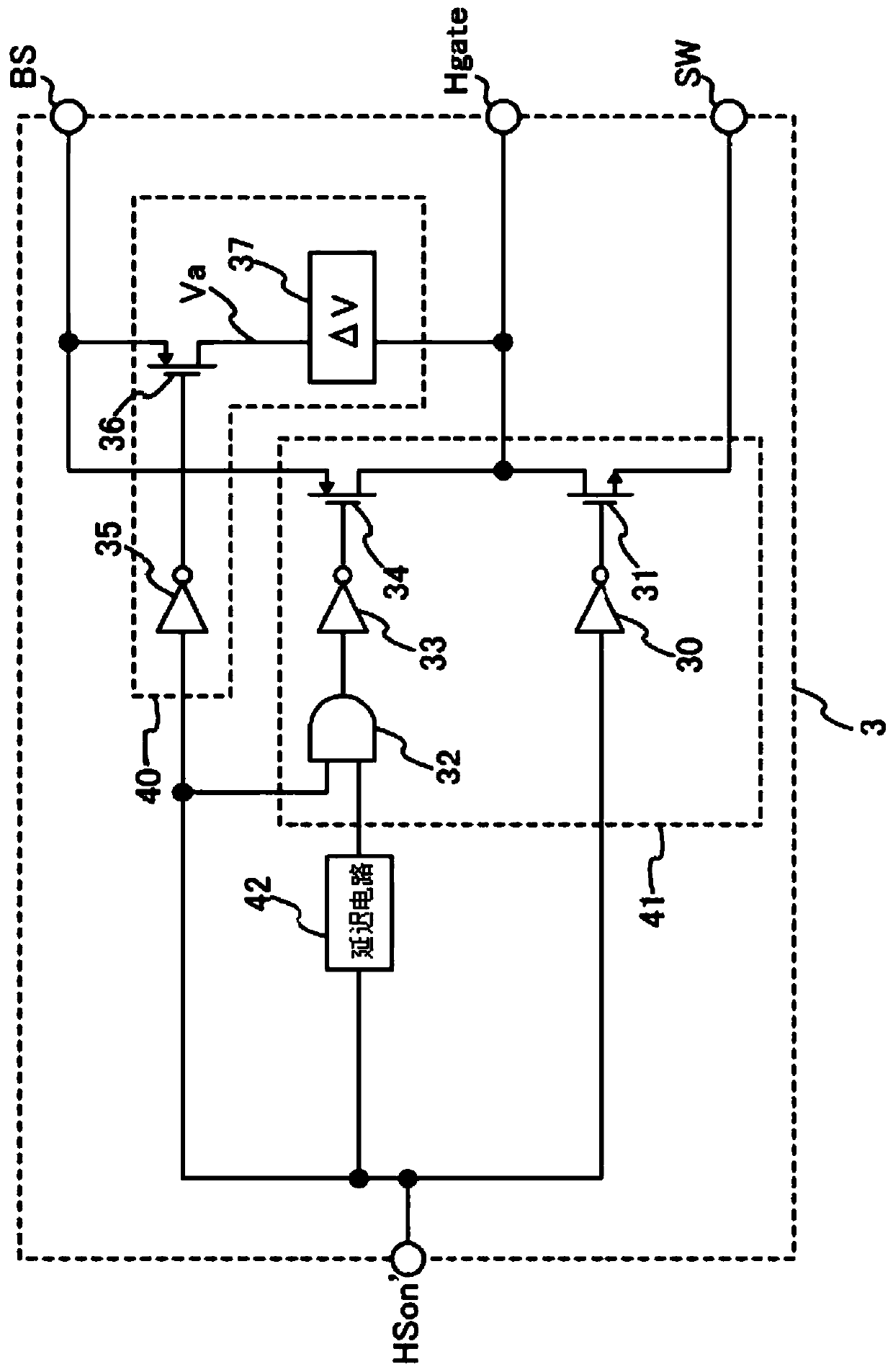
[0103] Figure 6 is shown as figure 2 A diagram of a circuit configuration of a high-side driver circuit 3 a of a modification example of the shown high-side driver circuit 3 . exist Figure 6 , the same reference numbers are assigned to the figure 2 The configuration shown is the same configuration, and a description thereof will not be presented.
[0104] In addition to replacing the sub-driver circuit 40 with a sub-driver circuit 40a, the high-side drive circuit 3a has the same figure 2 The high-side drive circuit 3 is shown in the same configuration.
[0105] The sub-drive circuit 40a has the same configuration as the sub-drive circuit 40 except that the voltage difference generating circuit 37 is replaced with a voltage difference generating circuit 37b, so only the voltage difference generating circuit 37b will be described. The voltage difference generating circuit 37b functions as a voltage generating circuit that generates the lowest driving voltage among the ...
no. 3 example
[0122] Figure 9 is shown as figure 2 A diagram of the circuit configuration of the high-side driver circuit 3b of the modification example of the high-side driver circuit 3 shown. exist Figure 9 , the same reference numbers are assigned to the figure 2 The configuration shown is the same configuration, and a description thereof will not be presented.
[0123] The high-side driver circuit 3 b has the same configuration as the high-side driver circuit 3 except that an on-detection circuit 43 is added.
[0124] The conduction detection circuit 43 includes an Nch-MOSFET 50 , a resistor 51 , and an inverter 52 configuring a current detection circuit that detects a current flowing through the high-side MOSFET 4 .
[0125] The gate terminal of Nch-MOSFET 50 is connected to the connection point between Nch-MOSFET 31 and Pch-MOSFET 34 . The source terminal of the Nch-MOSFET 50 is connected to the switch terminal SW, and the drain terminal of the Nch-MOSFET 50 is connected to o...
PUM
 Abstract
Description
Claims
Application Information


