Integrated chip crack detection device and method

A crack detection and integrated chip technology, applied in measurement devices, optical testing flaws/defects, instruments, etc., can solve the problems of inappropriate metal materials, inappropriate non-conductive materials, limited application value, etc., to improve reliability and reliability. Safety, improved spatial resolution, effect of eliminating noise components

Pending Publication Date: 2018-03-13
HARBIN INST OF TECH SHENZHEN GRADUATE SCHOOL
View PDF0 Cites 6 Cited by
  • Summary
  • Abstract
  • Description
  • Claims
  • Application Information

AI Technical Summary

Problems solved by technology

In recent years, some detection technologies have also been proposed, but their application value is limited due to their own technical reasons and the blankness of key technical content.
[0004] Overall, although many detection technologies for chip crack detection have been proposed so far, there are still key technical problems and defects that limit their development and practical engineering applications.
The disadvantages of the impact test technology listed above must be in contact with the target chip, which will cause potential damage to the chip; the strong eddy current used in the eddy current sensing technology will not only cause a certain degree of damage to the chip, but also affect its performance. effect, and this technique is not suitable for non-conductive materials
The terahertz wave in the terahertz imaging technology has a shallow penetration depth, and more importantly, it is not suitable for metal materials because it cannot penetrate the metal layer; although the scanning acoustic wave microscopy technology has a deeper penetration depth than the terahertz wave, However, due to its long detection time, it is not suitable for online detection. In addition, it is required that the target chip to be detected must be submerged in water or at least covered with water droplets, which may cause other damage to the chip.

Method used


Image

  • Integrated chip crack detection device and method
  • Integrated chip crack detection device and method
  • Integrated chip crack detection device and method

Examples


Embodiment Construction

[0046] It should be understood that the specific embodiments described here are only used to explain the present invention, not to limit the present invention.

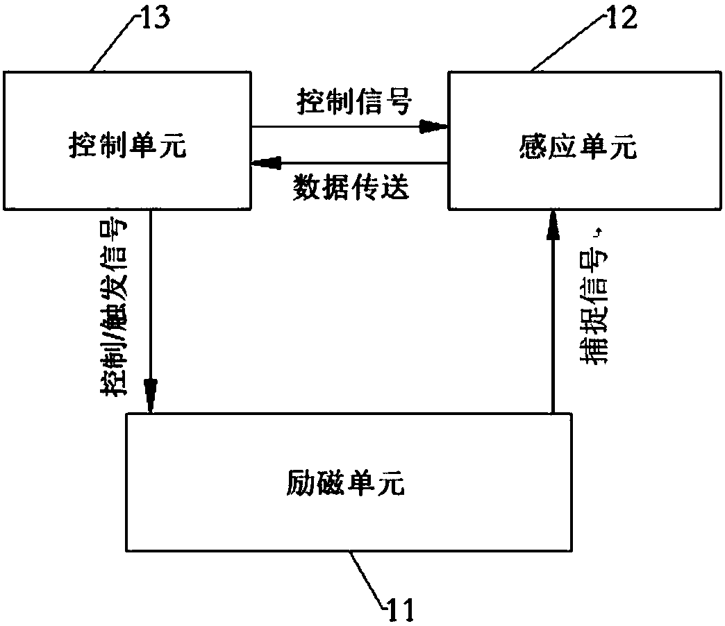
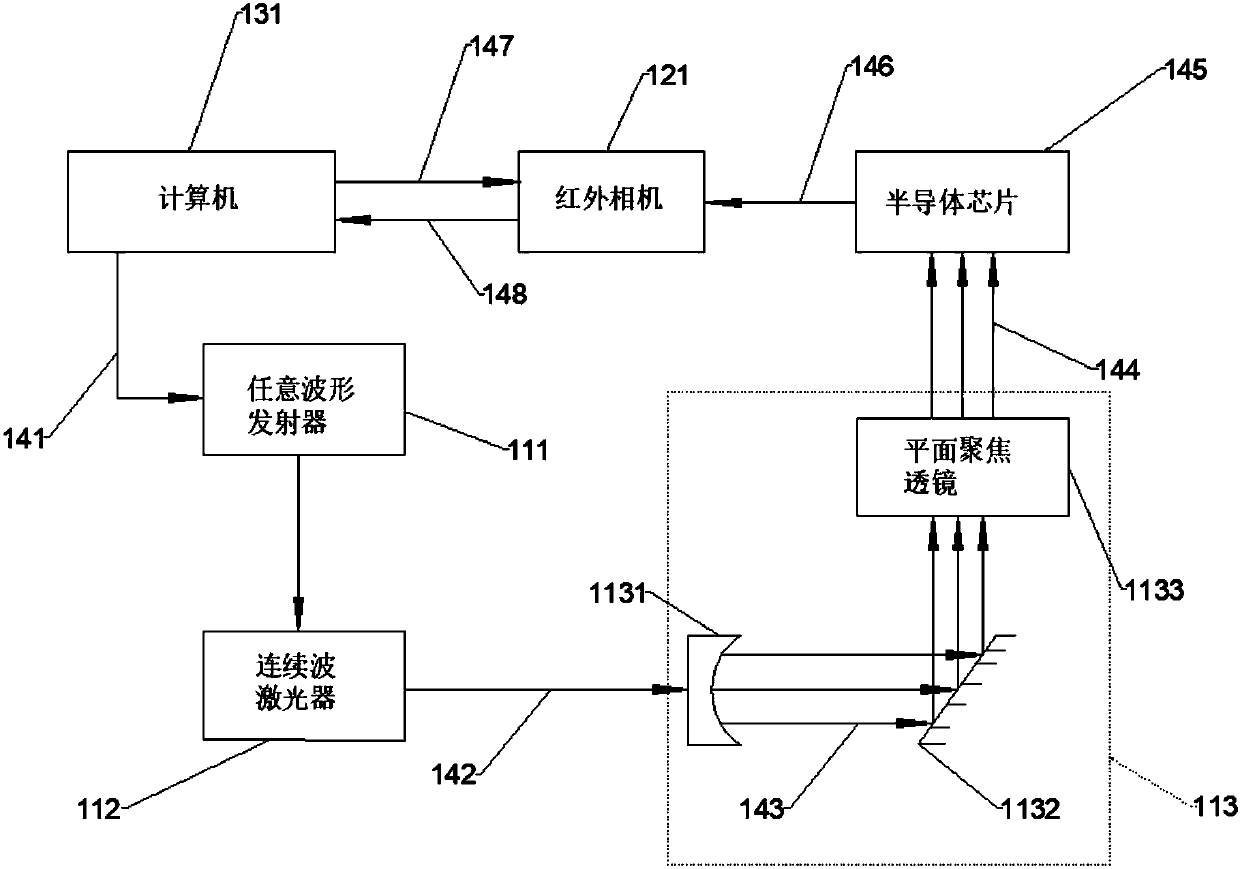
[0047] The integrated chip crack detection device of the present invention is based on the new line laser lock-in thermal imaging technology, which can achieve the following technological breakthroughs: (1) completely non-contact, non-damaging and non-invasive during detection; (2) not only can detect conductive materials, but also Applied to non-conductive materials; (3) Realize a self-developed visualization algorithm for chip cracks without baselines with intellectual property rights. Baseline-free crack diagnosis only requires thermal images of the current state and does not require any thermal images of historical states. The detection efficiency is high and it is suitable for online detection ; (4) The capability of crack detection is improved by improving the spatial resolution of the thermal image and eliminati...


PUM


Abstract

The invention discloses an integrated chip crack detection device and method. The device comprises: a control unit connected to each other, an induction unit, and an excitation unit. Under the instruction of the control unit, the excitation unit generates a linear laser beam, and the linear laser beam To the surface of the semiconductor chip, scan horizontally and vertically on the surface of the semiconductor chip, and at the same time, the linear laser beam generates a thermal wave at the desired excitation line, and the thermal response of the thermal wave is captured by the sensing unit, and the thermal response data is then transmitted to the control unit. The invention realizes non-contact, non-damage and non-intrusion detection and identification of cracks on the surface of the integrated chip; it is not limited by the chip material, has high detection efficiency, and is suitable for online detection; and improves the ability of crack detection and the reliability and safety of the integrated chip sex.

Description

technical field [0001] The invention relates to the field of integrated circuits, in particular to an integrated chip crack detection device and method. Background technique [0002] An integrated circuit, also known as a chip, is a miniature electronic device or component, generally a semiconductor material, known as the "heart" of industrial production. In the development and manufacturing process of chips, people's demand for lighter and thinner electronic products is increasing day by day. Therefore, manufacturers are required to manufacture smaller, thinner, and higher-performance integrated chips. However, the thinning of wafers for integrated chips has brought a series of problems. One of the main problems is the formation of defective products due to surface cracks during chip fabrication. There is a growing need to inspect integrated chips for surface cracks during the manufacturing process as surface cracks can degrade the performance and reliability of the fina...

Claims


Application Information

Patent Timeline
Patent Type & Authority Applications(China)
IPC IPC(8): G01N21/95
CPCG01N21/9505
Inventor 许颖陈锐柳成荫黄俊文罗聪聪
Owner HARBIN INST OF TECH SHENZHEN GRADUATE SCHOOL
Why Eureka
Try Eureka