795nm extreme-narrow linewidth external-cavity semiconductor laser

An ultra-narrow linewidth, semiconductor technology, applied in the field of semiconductor lasers, can solve the problems that lasers cannot meet the requirements of single-mode, high power, high beam quality, narrow linewidth, high coherence, wavelength tunable, etc. The effect of high power, high beam quality

Inactive Publication Date: 2018-03-16
NO 49 INST CHINESE ELECTRONICS SCI & TECH GRP
View PDF0 Cites 0 Cited by
  • Summary
  • Abstract
  • Description
  • Claims
  • Application Information

AI Technical Summary

Problems solved by technology

[0003] The present invention solves the problems that existing lasers are difficult to meet single-mode, high power, high beam quality, narrow linewidth, high coherence, and tunable wavelength, and provides a 795nm ultra-narrow linewidth external cavity semiconductor laser

Method used


Image

  • 795nm extreme-narrow linewidth external-cavity semiconductor laser
  • 795nm extreme-narrow linewidth external-cavity semiconductor laser
  • 795nm extreme-narrow linewidth external-cavity semiconductor laser

Examples


specific Embodiment approach 1

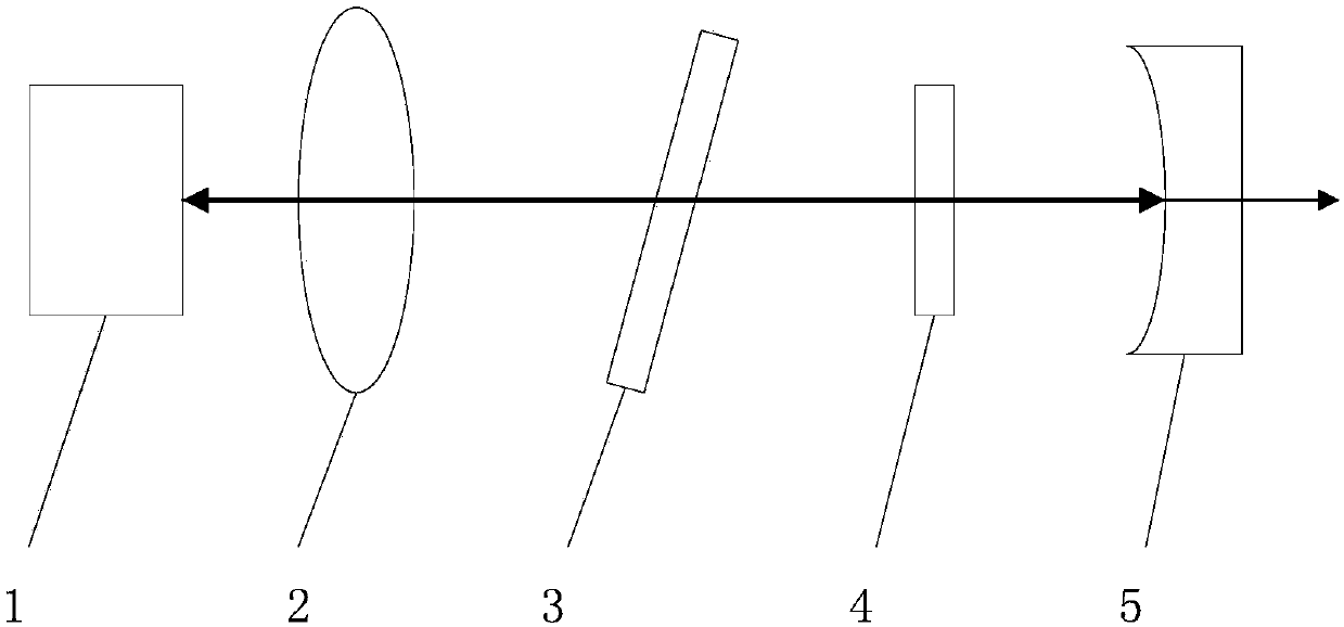
[0014] Specific implementation mode one: combine figure 1 and figure 2 Describe this embodiment in detail, a kind of 795nm ultra-narrow linewidth external cavity semiconductor laser of this embodiment is made of semiconductor laser gain chip 1, collimating lens 2, birefringent filter 3, Fabry-Perot etalon 4 and output coupling mirror 5 composition;

[0015] A collimating lens 2, a birefringent filter 3, a Fabry-Perot etalon 4 and an output coupling mirror 5 are sequentially provided on the light emitting direction of the semiconductor laser gain chip 1;

[0016] The emission wavelength of the semiconductor laser gain chip 1 is 795nm;

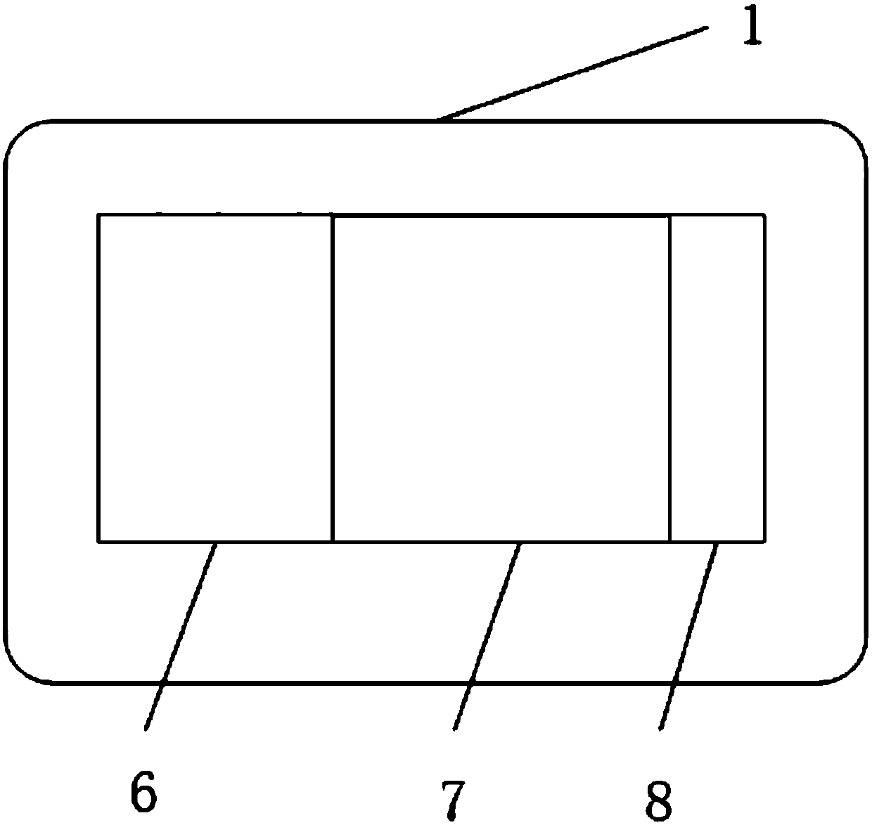
[0017] The semiconductor laser gain chip 1 includes a DBR mirror 6 , a gain region 7 and a window layer 8 .

[0018] The beneficial effects of this embodiment are:

[0019] Different from other narrow-linewidth lasers, this embodiment uses a birefringent filter and a Fabry-Perot etalon to perform linewidth compression simultaneously. The c...

specific Embodiment approach 2

[0020] Specific embodiment 2: The difference between this embodiment and specific embodiment 1 is that the collimator lens 2 is an aspheric mirror, the surface is coated with a 700nm-900nm anti-reflection coating, the numerical aperture is 0.5-0.6, and the effective focal length is 4.0 nm ~ 5.0mm. Others are the same as in the first embodiment.

specific Embodiment approach 3

[0021] Embodiment 3: This embodiment differs from Embodiment 1 or Embodiment 2 in that: the thickness of the birefringent filter 3 is 2mm, and the shape is a fan-shaped structure. Others are the same as in the first or second embodiment.


PUM


Abstract

A 795nm ultra-narrow line width external cavity semiconductor laser, the invention relates to a semiconductor laser. The invention aims to solve the problems that the existing lasers are difficult to meet single mode, high power, high beam quality, narrow line width, high coherence and tunable wavelength. A 795nm ultra-narrow linewidth external cavity semiconductor laser is composed of a semiconductor laser gain chip, a collimator lens, a birefringent filter, a Fabry-Perot etalon and an output coupling mirror; the light output direction of the semiconductor laser gain chip A collimating lens, a birefringent filter, a Fabry-Perot etalon and an output coupling mirror are sequentially arranged on the top; the emission wavelength of the semiconductor laser gain chip is 795nm; the semiconductor laser gain chip includes a DBR reflector , gain region and window layer. It can output narrow linewidth laser that meets application requirements, and its wavelength is linearly and continuously adjustable, meeting single-mode, high power, high beam quality and high coherence.

Description

technical field [0001] The present invention relates to a semiconductor laser. Background technique [0002] External cavity surface emitting semiconductor laser is a kind of surface emitting laser, which is a new type of device in semiconductor laser technology. Compared with edge-emitting semiconductor lasers, vertical external-cavity surface-emitting semiconductor lasers have a small divergence angle and do not need to shape the output beam. Compared with traditional solid-state lasers, they have the advantages of small size and high conversion efficiency. These characteristics make external cavity surface emitting semiconductor lasers have broad application prospects in the fields of laser display, laser communication, material processing, medical treatment and national defense. Ultra-narrow linewidth external cavity semiconductor lasers are widely used in the technical fields of quantum information, spectroscopy, coherent communication, remote sensing and precision mea...

Claims


Application Information

Patent Timeline
Patent Type & Authority Applications(China)
IPC IPC(8): H01S5/14H01S5/06
CPCH01S5/141H01S5/0607
Inventor 刘兴宇邵志强孙权桂勇雷崔洪亮邓崇杰
Owner NO 49 INST CHINESE ELECTRONICS SCI & TECH GRP
Why Eureka
Try Eureka