Laser based on semiconductor optical amplification chip

An optical amplification and semiconductor technology, applied in the field of semiconductor optical amplification chip lasers, to achieve the effect of realizing laser wavelength and enhancing mechanical stability

Inactive Publication Date: 2012-04-18
NAT TIME SERVICE CENT CHINESE ACAD OF SCI
View PDF5 Cites 0 Cited by
  • Summary
  • Abstract
  • Description
  • Claims
  • Application Information

AI Technical Summary

Problems solved by technology

This method needs the laser and the semiconductor optical amplifier to be used together, which is not only costly, but also unstable and prone to failure.

Method used


Image

  • Laser based on semiconductor optical amplification chip
  • Laser based on semiconductor optical amplification chip

Examples


Embodiment 1

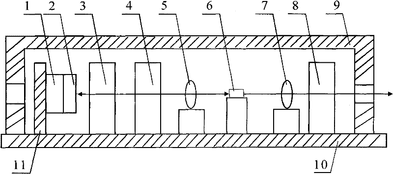
[0016] exist figure 1 Among them, the laser device based on the semiconductor optical amplification chip of the present embodiment consists of a piezoelectric transducer 1, a total reflection mirror 2, a focusing lens 3, a mode selection device 4, a first collimating lens 5, a semiconductor optical amplification chip 6, a second A collimator lens 7, a cylindrical lens 8, a cover body 9, a base plate 10, and a support block 11 are connected to form.

[0017] The base plate 10 is fixedly connected with a cover body 9 with a threaded fastening connector, and a wire hole is processed on the left side wall of the cover body 9, and the wire can pass through the wire hole, and a light exit hole is processed on the right side wall of the cover body 9 , the laser can be emitted through the light hole. The left side of the inner bottom plate 10 of the cover body 9 is fixedly connected with a support block 11 with a threaded fastener, and a piezoelectric transducer 1 is fixedly connect...

Embodiment 2

[0019] The anti-reflection film on the incident surface of the semiconductor optical amplifier chip 6 of the present embodiment is vacuum alternately vaporized 8 layers of silicon dioxide and zirconium dioxide, and the partial reflection film on the outgoing surface of the semiconductor optical amplifier chip 6 is vacuum alternately deposited 14 layers of fluoride. Magnesium and Calcium Fluoride. 24 layers of aluminum oxide and tantalum pentoxide reflection films are alternately vacuum-evaporated on the mirror surface of the total reflection mirror 2 . The mode selection device 4 is a Fabry-Perot etalon with a bandwidth of less than 200 GHz and a transmittance of 80%. The other components of this embodiment and the coupling relationship of the components are the same as those of Embodiment 1.

Embodiment 3

[0021] The anti-reflection film on the incident surface of the semiconductor optical amplifier chip 6 of this embodiment is vacuum alternately vaporized 12 layers of silicon dioxide and zirconium dioxide, and the partial reflection film on the outgoing surface of the semiconductor optical amplifier chip 6 is vacuum alternately deposited 18 layers of fluoride Magnesium and Calcium Fluoride. 30 layers of aluminum oxide and tantalum pentoxide reflective films are vacuum-evaporated alternately on the mirror surface of the total reflection mirror 2 . The mode selection device 4 is a Fabry-Perot etalon with a bandwidth of less than 200 GHz and a transmittance of 80%. The other components of this embodiment and the coupling relationship of the components are the same as those of Embodiment 1.


PUM


Abstract

The invention relates to a laser based on a semiconductor optical amplification chip. A soleplate is provided with a cover body, a lead hole is processed on the left lateral wall of the cover body, a light-emitting hole is processed on the right lateral wall of the cover body, the left side of the soleplate in the cover body is provided with a supporting block provided with a piezoelectric transducer the right side of which is provided with a total reflector, the total reflector on the soleplate is provided with a focusing lens in the right horizontal optical axis direction, the focusing lensis provided with a mode selecting device in the right horizontal optical axis direction, the mode selecting device is provided with a first collimating lens in the right horizontal optical axis direction, the first collimating lens is provided with a semiconductor optical amplification chip in the right horizontal optical axis direction; and the incoming surface of the semiconductor optical amplification chip is coated with a reflection reducing film, the outgoing surface of the semiconductor optical amplification chip is coated with a reflecting film, the semiconductor optical amplification chip is provided with a second collimating lens in the right horizontal optical axis direction, and the second collimating lens is provided with a cylinder lens in the right horizontal optical axis direction.

Description

technical field [0001] The invention belongs to the field of semiconductor lasers, in particular to a semiconductor optical amplifier chip laser. Background technique [0002] The semiconductor optical amplifier chip is a device that can realize optical power amplification. It has the characteristics of miniaturization, low power consumption and high gain, and the gain factor can reach 30dB. It has a wide range of applications in long-distance optical fiber communication, cold atoms and other fields that require high-power lasers (greater than 500mW). However, the semiconductor optical amplifier chip cannot be used alone. A laser is required to provide seed light and inject it into the current-loaded chip gain medium to realize the power amplification of the seed light while keeping the output laser characteristics unchanged. In the case of no seed laser input, the light output by the semiconductor optical amplifier chip is not laser, but ordinary natural light. This meth...

Claims


Application Information

Patent Timeline
Patent Type & Authority Patents(China)
IPC IPC(8): H01S5/10H01S5/30
Inventor 阮军张首刚吴长江张辉刘杰刘丹丹
Owner NAT TIME SERVICE CENT CHINESE ACAD OF SCI
Why Eureka
Try Eureka