Multi-wavelength ring laser chip

A ring laser, multi-wavelength technology, used in lasers, laser parts, phonon exciters, etc., to solve the problem of on-chip optical signal amplification, convenient manufacturing, high reliability and environmental adaptability

Pending Publication Date: 2022-04-15
SHANGHAI AEROSPACE SCI & IND ELECTRIC APPLIANCE RES INST
View PDF9 Cites 0 Cited by
  • Summary
  • Abstract
  • Description
  • Claims
  • Application Information

AI Technical Summary

Problems solved by technology

The on-chip integrated frequency multiplier, modulator, filter, and passive active optical waveguide of lithium niobate thin film have been successfully developed, but the on-chip integrated communication band light source is still in urgent need of research

Method used


Image

  • Multi-wavelength ring laser chip
  • Multi-wavelength ring laser chip
  • Multi-wavelength ring laser chip

Examples


Embodiment Construction

[0030] The present invention will be further explained below in conjunction with specific embodiments.

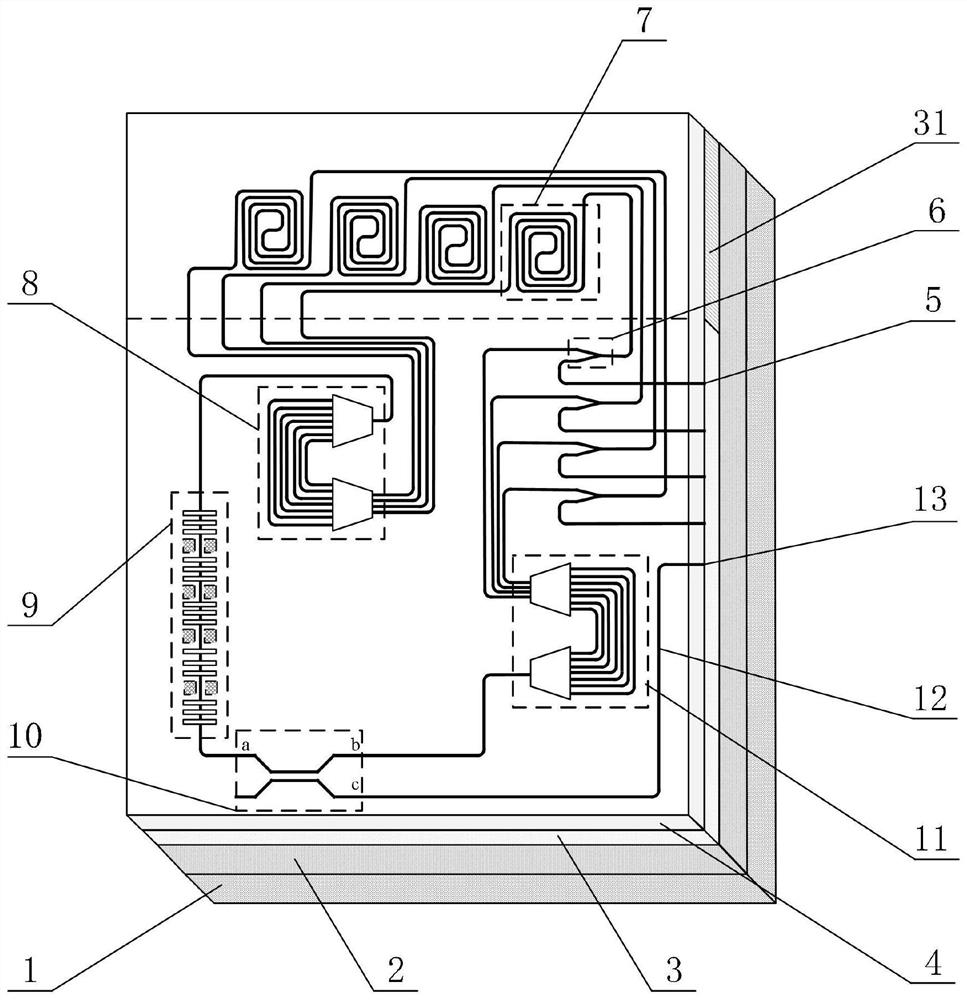
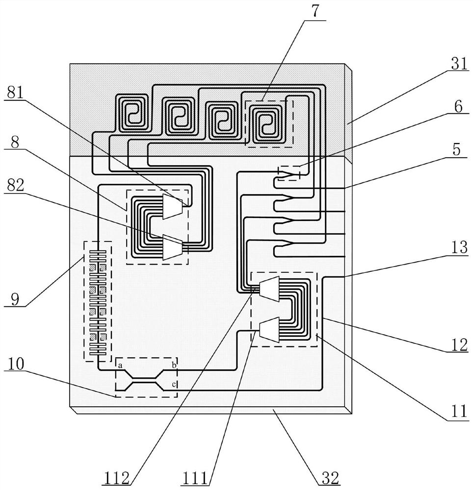
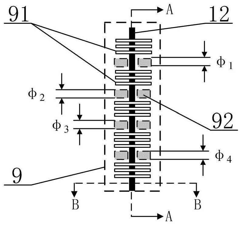
[0031] refer to Figure 1-9 , a multi-wavelength ring laser chip, comprising a chip substrate 1, the upper surface of the chip substrate 1 is successively provided with a chip lower cladding layer 2 and a chip upper cladding layer 4, and between the chip lower cladding layer 2 and the chip upper cladding layer 4 The core layer 3, the core layer 3 is spliced ​​by the active waveguide core layer 31 and the passive waveguide core layer 32, the material of the active waveguide core layer 31 is an erbium-doped lithium niobate single crystal film, the passive waveguide core layer 32 The material is lithium niobate single crystal thin film. The thickness of the erbium-doped lithium niobate single crystal thin film and the lithium niobate single crystal thin film is 700nm. The chip substrate 1 is made of lithium niobate or silicon, and the chip lower cladding layer 2 and the chip...


PUM


Abstract

The invention discloses a multi-wavelength ring laser chip which comprises a chip substrate, a chip lower wrapping layer, a passive waveguide core layer and an active waveguide core layer. A periodic wavelength selection function of the array waveguide grating is utilized, the array waveguide grating, a plurality of active waveguide amplifiers and a tunable filter are subjected to monolithic integration, so that a corresponding multi-wavelength and wavelength-tunable light source is obtained, and the scheme can generate stable and synchronous multi-wavelength oscillation under the condition of no complex wavelength control; the multi-wavelength laser chip not only meets the wavelength requirement of a wavelength division multiplexing communication band, but also has the greater advantages of being high in integration level, small in size, tunable in wavelength, and high in reliability and environmental adaptability.

Description

technical field [0001] The invention relates to the technical field of wavelength division multiplexing communication multi-wavelength light sources, in particular to a multi-wavelength ring laser chip. Background technique [0002] The wavelength division multiplexing optical fiber communication system organically combines optical wavelength division multiplexing technology with optical fiber communication, improves communication capacity while signal transmission, and solves the problem of low utilization rate of optical fiber communication. In the wavelength division multiplexing communication system, the multi-wavelength light source is a very important part, especially the multi-wavelength light source with equal wavelength interval and flat power. At present, the light source commonly used in communication systems uses semiconductor distributed feedback laser arrays, and then couples the output wavelengths of different lasers to the same optical fiber to form a multi-w...

Claims


Application Information

Patent Timeline
Patent Type & Authority Applications(China)
IPC IPC(8): H01S3/08H01S3/094
Inventor 李贝陈宏志曹军
Owner SHANGHAI AEROSPACE SCI & IND ELECTRIC APPLIANCE RES INST
Why Eureka
Try Eureka