Protective film for chip cutting as well as preparation method and use method thereof

A technology for protective films and chips, applied in pressure-sensitive films/sheets, film/sheet-like adhesives, adhesive types, etc. The effect of small time change, high weather resistance and high material strength

Inactive Publication Date: 2018-03-20
CYBRID TECHNOLOGIES INC
View PDF6 Cites 11 Cited by
  • Summary
  • Abstract
  • Description
  • Claims
  • Application Information

AI Technical Summary

Problems solved by technology

However, the base material of PVC-based protective film is PVC material, and PVC material contains halogen, which does not meet environmental protection requirements such as ROHS, has environmental safety hazards, and is strictly restricted in many areas; Molecular Contamination Components

Method used


Image

  • Protective film for chip cutting as well as preparation method and use method thereof
  • Protective film for chip cutting as well as preparation method and use method thereof

Examples


Embodiment 1

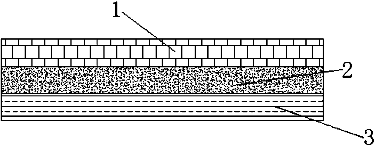
[0030] Such as figure 1 As shown, a protective film for chip dicing in this embodiment includes a release layer 1, a substrate layer 2 and an adhesive layer 3 in sequence, the substrate layer 2 is made of a modified PO material, and the modified PO material is made of PP and PE Copolymerized, the modified PO material includes, by weight, 50 parts of PP, 40 parts of PE, and 10 parts of talcum powder.

[0031] Wherein, the substrate layer 2 is a three-layer co-extruded structure, the thickness of the substrate layer 2 is 50 μm, including an inner layer, a core layer and an outer layer respectively made of a modified PO material, the thickness of the inner layer is 5 μm, and the thickness of the core layer is 5 μm. The thickness is 40 μm, and the thickness of the outer layer is 5 μm. The strength of the substrate layer 2 is 20N / mm 2 . The modified PO material of the inner layer also includes 0.5 parts by weight of a strong polar additive, which can improve the adhesion between...

Embodiment 2

[0044] Such as figure 1 As shown, a protective film for chip dicing in this embodiment includes a release layer 1, a substrate layer 2 and an adhesive layer 3 in sequence, the substrate layer 2 is made of a modified PO material, and the modified PO material is made of PP and PE Copolymerized, the modified PO material includes, by weight, 70 parts of PP, 20 parts of PE, and 10 parts of talcum powder.

[0045] Wherein, the substrate layer 2 is a three-layer co-extruded structure, the thickness of the substrate layer 2 is 100 μm, including an inner layer, a core layer and an outer layer respectively made of a modified PO material, the thickness of the inner layer is 10 μm, and the thickness of the core layer is 100 μm. The thickness is 80 μm, and the thickness of the outer layer is 10 μm. The strength of the substrate layer 2 is 50N / mm 2 . The modified PO material of the inner layer also includes 2 parts by weight of a strong polar additive, which can improve the adhesion betw...

Embodiment 3

[0053] Such as figure 1 As shown, a protective film for chip dicing in this embodiment includes a release layer 1, a substrate layer 2 and an adhesive layer 3 in sequence, the substrate layer 2 is made of a modified PO material, and the modified PO material is made of PP and PE Copolymerized, the modified PO material includes, by weight, 60 parts of PP, 35 parts of PE, and 5 parts of talcum powder.

[0054] Wherein, the substrate layer 2 is a three-layer co-extruded structure, the thickness of the substrate layer 2 is 80 μm, including an inner layer, a core layer and an outer layer respectively made of a modified PO material, the thickness of the inner layer is 10 μm, and the thickness of the core layer is 10 μm. The thickness is 60 μm, and the thickness of the outer layer is 10 μm. The strength of the substrate layer 2 is 40N / mm 2 . The modified PO material of the inner layer also includes 1.5 parts by weight of a strong polar additive, which can improve the adhesion betwe...


PUM

PropertyMeasurementUnit
thicknessaaaaaaaaaa
strengthaaaaaaaaaa
thicknessaaaaaaaaaa

Abstract

The invention discloses a protective film for chip cutting. The protective film sequentially comprises a releasing layer, a substrate layer and an adhesive layer, wherein the substrate layer is made of modified PO (propylene epoxide) material; the modified PO material is prepared by copolymerizing PP (polypropylene) and PE (polyethylene); the modified PO material is prepared from the following components in parts by weight: 50 to 70 parts of PP, 20 to 40 parts of PE, and 5 to 10 parts of talcum powder. The protective film has the characteristics that the substrate layer adopts the modified POmaterial, so that the mechanical strength is high, the halogen is avoided, and the environment-friendly requirement is met; the heat-resistant property is better, and the certain high-temperature operation requirement is met; the plasticizer is not contained, so that the risk of micromolecule segregation is avoided for the material; the material strength is high, the ductility is good, the uniformshrinkage rate in each direction is maintained under the condition of 140% of elongation rate, and the uniform strength in each direction is realized at the premises of certain elongation rate; the adhesive layer uses pressure-sensitive adhesive to replace the photo-sensitive adhesive and thermo-sensitive adhesive, the transparency degree is high, the weather-resistant property is high, TG is about -20 DEG C, and the procedures are simple (no UV (ultraviolet) furnace passing or reheating procedure); by performing simple laminating and separating, the product application requirement can be met, the change of viscosity duration is small and is less than 20%, and the residual adhesive is avoided.

Description

technical field [0001] The invention relates to the technical field of protective films, in particular to a protective film for chip dicing, a preparation method and a use method thereof. Background technique [0002] With the rapid growth of the semiconductor industry, the supporting materials have attracted the attention of the industry. The process of semiconductor products can be divided into: chip design, chip manufacturing, packaging and testing. Among them, a cutting protective film is used in the packaging and testing process. The function of this material is to effectively separate the cut chips for subsequent pick-up and packaging operations. [0003] At present, the encapsulation process of semiconductor products after dicing uses PVC-based protective films, and the product structure is backside treatment layer / PVC layer / adhesive layer. The feature of this product is that it meets the cutting process, and the tensile length of the material in all directions (360...

Claims


Application Information

Patent Timeline
Patent Type & Authority Applications(China)
IPC IPC(8): C09J7/24C09J7/29C09J7/38C09J133/08C09J11/06C08L23/12C08L23/06C08K3/34H01L23/29
CPCC08K3/34C08K5/1345C08L23/06C08L23/12C09J11/06C09J133/064C09J2301/162C09J2423/046C09J2423/106C09J2433/00H01L23/293
Inventor 李阜阳沈秦飞陈洪野吴小平
Owner CYBRID TECHNOLOGIES INC
Why Eureka
Try Eureka