
Electron static discharge (ESD) clamping circuit and integrated circuit

A clamping circuit and circuit technology, applied in the direction of circuits, electrical components, electric solid devices, etc., can solve the problem of occupying a large layout area, and achieve the effect of increasing the equivalent resistance, reducing the capacitance C, and reducing the layout area

Active Publication Date: 2018-03-30
INST OF MICROELECTRONICS CHINESE ACAD OF SCI
View PDF6 Cites 3 Cited by
  • Summary
  • Abstract
  • Description
  • Claims
  • Application Information

AI Technical Summary

Problems solved by technology

[0006] By providing an ESD clamping circuit and an integrated circuit, the present invention solves the technical problem that the clamping circuit used for electrostatic protection in the prior art occupies an excessively large layout area

Method used


Image

  • Electron static discharge (ESD) clamping circuit and integrated circuit
  • Electron static discharge (ESD) clamping circuit and integrated circuit
  • Electron static discharge (ESD) clamping circuit and integrated circuit

Examples


Embodiment 1

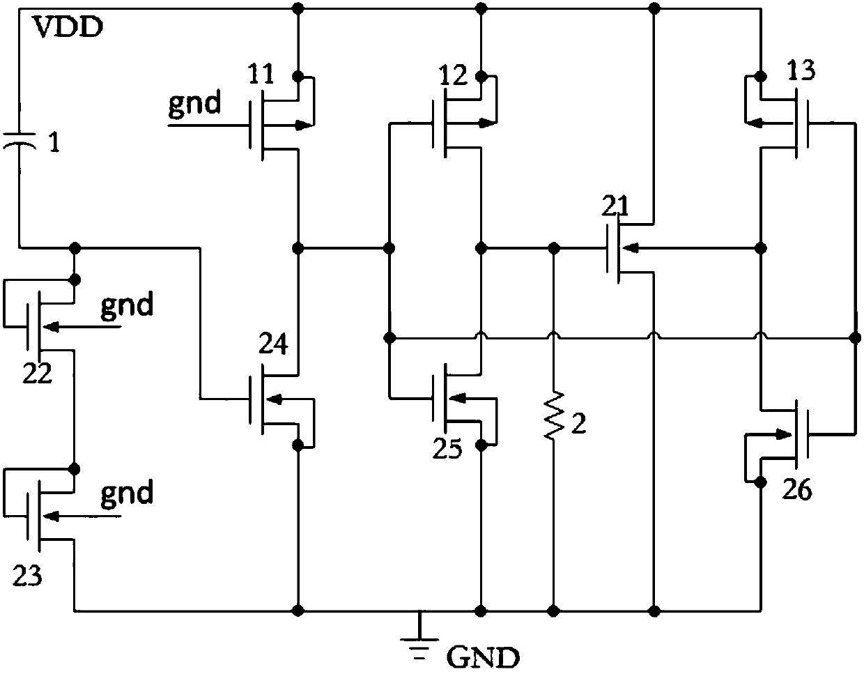
[0039] In this embodiment, an ESD clamping circuit is provided, such as figure 2 Shown include:

[0040] Capacitor 1, resistor 2, first P-type transistor 11, second P-type transistor 12, third P-type transistor 13, first N-type transistor 21, second N-type transistor 22, third N-type transistor 23, fourth N-type transistor 24, fifth N-type transistor 25 and sixth N-type transistor 26;

[0041] Wherein, the source of the first P-type transistor 11 is connected to the power supply VDD, the drain of the first P-type transistor 11 is connected to the gate of the second P-type transistor 12, and the first P-type transistor 11 The gate of the second P-type transistor 12 is connected to the power supply, and the drain of the second P-type transistor 12 is connected to the gate of the first N-type transistor 21; the third P The source of the third P-type transistor 13 is connected to the power supply, the drain of the third P-type transistor 13 is connected to the drain of the sixt...

Embodiment 2

[0054] This embodiment provides an integrated circuit, such as Figure 5 shown, including:

[0055] A functional circuit 501 and a clamping circuit 502 connected to the functional circuit 501;

[0056] The clamping circuit 502 includes: a capacitor, a resistor, a first P-type transistor, a second P-type transistor, a third P-type transistor, a first N-type transistor, a second N-type transistor, a third N-type transistor, a fourth N-type transistors, fifth N-type transistors and sixth N-type transistors;

[0057] Wherein, the source of the first P-type transistor is connected to a power supply, the drain of the first P-type transistor is connected to the gate of the second P-type transistor, and the gate of the first P-type transistor is grounded; The source of the second P-type transistor is connected to the power supply, and the drain of the second P-type transistor is connected to the gate of the first N-type transistor; the source of the third P-type transistor is connec...


PUM

PropertyMeasurementUnit
Capacitanceaaaaaaaaaa

Abstract

The invention discloses an electron static discharge (ESD) clamping circuit and an integrated circuit. The clamping circuit comprises a capacitor, a resistor, a first P-type transistor, a second P-type transistor, a third P-type transistor, a first N-type transistor, a second N-type transistor, a third N-type transistor, a fourth N-type transistor, a fifth N-type transistor and a sixth N-type transistor, wherein a source of the second N-type transistor is connected with a drain of the third N-type transistor, the capacitor is connected between the drain of the second N-type transistor and a power supply, a gate of the second N-type transistor is connected with the drain of the second N-type transistor, a source of the third N-type transistor is connected with ground, and a gate of the third N-type transistor is connected with a drain of the third N-type transistor. With the circuit provided by the invention, the technical problem of excessively large occupied layout area of the clamping circuit for electrostatic protection in the prior art is solved, and the technical effect of reducing the layout area is achieved.

Description

technical field [0001] The invention relates to the field of semiconductors, in particular to an ESD clamping circuit and an integrated circuit. . Background technique [0002] With the advancement of integrated circuit technology, the feature size of Metal-Oxide-Semiconductor Field-Effect Transistor (MOSFET) is getting smaller and smaller, and the thickness of the gate oxide layer is getting thinner. Under the trend, it is very important to use a high-performance electrostatic discharge (Electron Static Discharge, ESD) protection device to discharge electrostatic charges to protect the gate oxide layer. . When the electrostatic discharge of the integrated circuit will generate hundreds or even thousands of volts of high voltage, the gate oxide layer of the input stage in the integrated circuit will be broken down. In order to be able to withstand such a high ESD voltage, integrated circuit products usually must use ESD protection devices with high performance and high en...

Claims


Application Information

Patent Timeline
IPC IPC(8): H01L27/02
CPCH01L27/0266H01L27/0296
Inventor 蔡小五罗家俊刘海南陆江曾传滨卜建辉赵海涛
Owner INST OF MICROELECTRONICS CHINESE ACAD OF SCI
Learn More