Hf<x>Si<1-x>O2 multi-component oxide storage material-based charge storage device and fabrication method thereof

A technology of charge storage and storage materials, which is applied in the direction of electric solid-state devices, electrical components, semiconductor devices, etc., can solve the problems of increased leakage current, low charge storage density, and reduced thickness, so as to reduce the probability of electron leakage, Effect of improving charge retention ability and reducing charge loss

Inactive Publication Date: 2018-03-30
ANYANG NORMAL UNIV
View PDF7 Cites 0 Cited by
  • Summary
  • Abstract
  • Description
  • Claims
  • Application Information

AI Technical Summary

Problems solved by technology

However, this type of structure has the following disadvantages: 1) the tunneling layer SiO 2 The thickness keeps decreasing, the leakage current increases, and the power consumption of the device is serious; 2) the storage layer Si 3 N 4 The trap state density is not high, and the charge storage density is low; 3) the storage layer Si 3 N 4 The defect states have complex energy level distribution, and some of the charges trapped by the shallow energy level defect states are easy to escape, resulting in a decrease in device reliability.
[0003] In order to solve the above problems, multiple oxide materials are used instead of Si 3 N 4 Improving the defect state density of the structure has become a research hotspot, while the research on tunneling layer and barrier layer is less

Method used


Image

  • Hf&lt;x&gt;Si&lt;1-x&gt;O2 multi-component oxide storage material-based charge storage device and fabrication method thereof
  • Hf&lt;x&gt;Si&lt;1-x&gt;O2 multi-component oxide storage material-based charge storage device and fabrication method thereof
  • Hf&lt;x&gt;Si&lt;1-x&gt;O2 multi-component oxide storage material-based charge storage device and fabrication method thereof

Examples


Embodiment 1

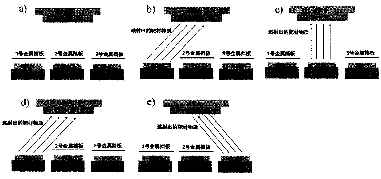
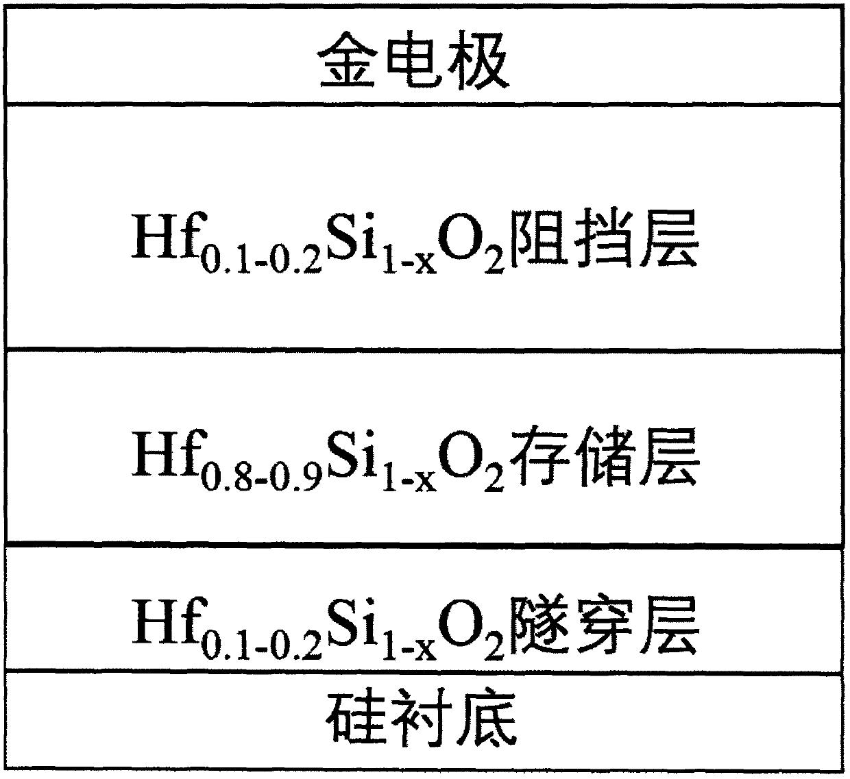
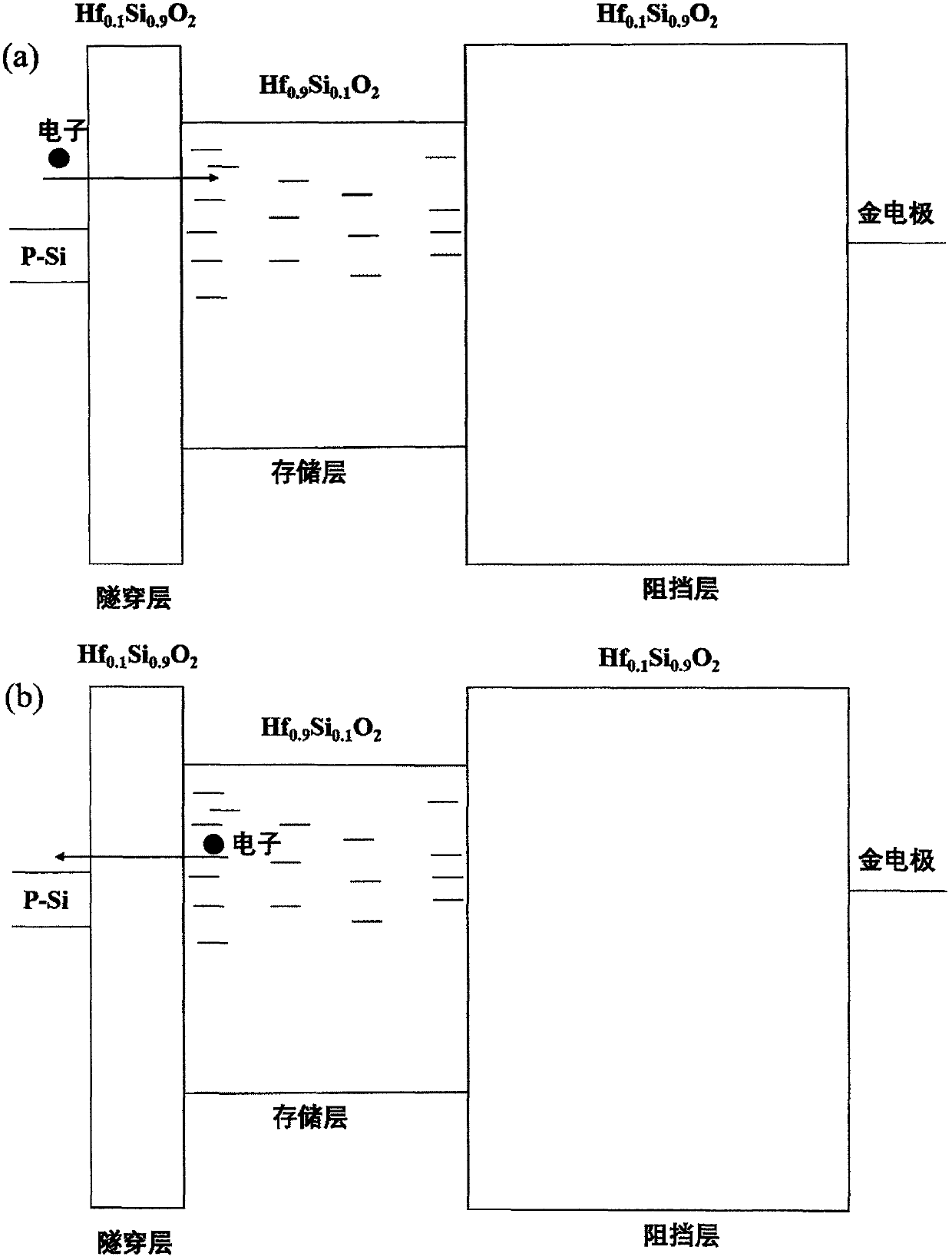
[0025] Embodiment 1: Based on p-Si substrate, prepare p-Si / Hf by means of magnetron sputtering 0.1 Si 0.9 o 2 / Hf 0.9 Si 0.1 o 2 / Hf 0.1 Si 0.9 o 2 / Au charge trap memory device fabrication process is as follows:

[0026] a) Put the silicon substrate into an appropriate amount of acetone, ultrasonically clean it, then ultrasonically clean it with deionized water, then place it in a dilute hydrogen fluoride solution to remove surface oxides, and then put it into the lining in the three-target magnetron sputtering deposition chamber On the bottom platform, prepare to grow a film on the surface; the Hf 0.1 Si 0.9 o 2 and Hf 0.9 Si 0.1 o 2 The ceramic targets were placed on the No. 1 and No. 2 target stages of the magnetron sputtering deposition chamber, and the gold target was placed on the No. 3 target stage. The temperature of the substrate stage was 300 ° C, and the vacuum in the cavity was 1 × 10 -4 Pa:

[0027] b) Use the metal baffle to block the ceramic targ...

Embodiment 2

[0032] Embodiment 2: Based on p-Si substrate, prepare p-Si / Hf by means of magnetron sputtering 0.1 Si 0.9 o 2 / HfO 2 / Hf 0.1 Si 0.9 o 2 / Au charge trap memory device fabrication process is as follows:

[0033] a) Put the silicon substrate into an appropriate amount of acetone, ultrasonically clean it, then ultrasonically clean it with deionized water, then place it in a dilute hydrogen fluoride solution to remove surface oxides, and then put it into the lining in the three-target magnetron sputtering deposition chamber On the bottom platform, prepare to grow a film on the surface; the Hf 0.1 Si 0.9 o 2 and HfO 2 The ceramic targets were placed on the No. 1 and No. 2 target stages of the magnetron sputtering deposition chamber, and the gold target was placed on the No. 3 target stage. The temperature of the substrate stage was 300 ° C, and the vacuum in the cavity was 1 × 10 -4 Pa;

[0034] b) Use the metal baffle to block the ceramic targets and gold targets on the ...

Embodiment 3

[0039] Example 3: Preparation of p-Si / SiO by magnetron sputtering based on p-Si substrate 2 / Hf 0.9 Si 0.1 o 2 / SiO 2 / Au charge trap memory device fabrication process is as follows:

[0040]a) Put the silicon substrate into an appropriate amount of acetone, ultrasonically clean it, then ultrasonically clean it with deionized water, then place it in a dilute hydrogen fluoride solution to remove surface oxides, and then put it into the lining in the three-target magnetron sputtering deposition chamber On the bottom platform, prepare to grow thin films on the surface; SiO 2 and Hf 0.9 Si 0.1 o 2 The ceramic targets were placed on the No. 1 and No. 2 target stages of the magnetron sputtering deposition chamber, and the gold target was placed on the No. 3 target stage. The temperature of the substrate stage was 300 ° C, and the vacuum in the cavity was 1 × 10 -4 Pa;

[0041] b) Use the metal baffle to block the ceramic targets and gold targets on the No. 2 and No. 3 targe...


PUM

PropertyMeasurementUnit
Thicknessaaaaaaaaaa
Thicknessaaaaaaaaaa
Thicknessaaaaaaaaaa

Abstract

The invention discloses an Hf<x>Si<1-x>O2 charge storage material. A method for fabricating a charge storage device by employing magnetron sputtering can be used for a non-volatile information storagedevice. The method comprises the steps of placing a silicon substrate on a three-target magnetron sputtering substrate table, and sequentially growing an Hf<0.1-0.2>Si<1-x>O2 tunneling layer, an Hf<0.8-0.9>Si<1-x>O2 storage layer, an Hf<0.1-0.2>Si<1-x>O2 blocking layer and a gold electrode on a surface of the silicon substrate by magnetron sputtering to form the charge storage device.

Description

technical field [0001] The invention belongs to the field of microelectronic devices and materials thereof, and relates to a Hf x Si 1-x o 2 Multiple oxide charge storage materials and their applications in nonvolatile charge storage devices. Background technique [0002] With the gradual shrinking of the feature size of semiconductor devices and the continuous improvement of integration, the traditional floating gate non-volatile memory devices have been difficult to meet the market demand. In recent years, metal (Metal)-silicon dioxide (SiO 2 )-Silicon Nitride (Si 3 N 4 )-Silicon dioxide (SiO 2 )-Silicon substrate (Si) type (MONOS) charge memory becomes a candidate structure to replace the floating gate type memory. The main feature of the MONOS charge memory structure is the use of Si 3 N 4 Replace the polysilicon floating gate in the traditional floating gate structure to store charges; SiO next to the silicon substrate 2 As a tunneling layer, SiO next to the m...

Claims


Application Information

Patent Timeline
IPC IPC(8): H01L27/11568
CPCH10B43/30
Inventor 汤振杰李荣张希威
Owner ANYANG NORMAL UNIV
Why Eureka
Try Eureka