Waveguide-coupled semiconductor laser

A laser and semiconductor technology, applied in the field of lasers, can solve the problems that do not conform to the development trend of miniaturization and the large volume of lasers, and achieve the effects of simple processing, high-power laser output, and low production cost

Inactive Publication Date: 2018-04-03
FUZHOU PHOTOP QPTICS CO LTD
View PDF7 Cites 0 Cited by
  • Summary
  • Abstract
  • Description
  • Claims
  • Application Information

AI Technical Summary

Problems solved by technology

The structure of existing high-power lasers generally includes an LD array stack, a fiber coupling system, and a fiber combiner. Due to the large volume of the fiber combiner, the volume of the formed laser is relatively large, which does not meet the development trend of miniaturization.

Method used


Image

  • Waveguide-coupled semiconductor laser
  • Waveguide-coupled semiconductor laser
  • Waveguide-coupled semiconductor laser

Examples


Embodiment 1

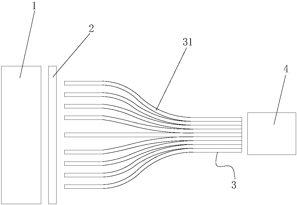
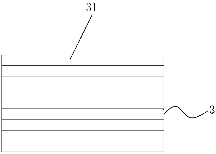
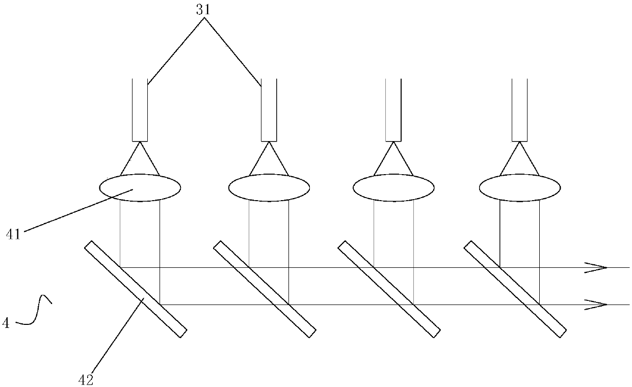
[0021] Example 1, such as figure 1 or figure 2 As shown, the light output ends of the waveguide sheets 31 are closely attached to each other sequentially, so as to realize the beam combining of the output light. In order to further improve the beam combining effect of the output light, an optical beam combining system 4 may also be provided on the side of the light output end of the waveguide coupler 3, and the optical beam combining system 4 may be a block grating. or as image 3 As shown, the optical beam combining system 4 can also be a collimator lens 41 and a WDM diaphragm 42 sequentially arranged on the light output side of each waveguide sheet 31, and the inclination angles of each WDM diaphragm 42 are the same.

[0022] In addition, as an optimization, an FBG grating can be etched on the light output end of the waveguide sheet 31 for locking the wavelength.

[0023] The working principle of this example 1: the optical input ends of each waveguide sheet 31 are coupl...

Embodiment 2

[0025] The structure and principle of embodiment 2 and embodiment 1 are basically the same, as Figure 4 or Figure 5 As shown, the difference is that the light output ends of the waveguide sheets 31 are not tightly attached together in sequence, but there are gaps between them. Due to the existence of gaps, the beam combining effect of the output light is worse than that of Embodiment 1, so an optical beam combining system 4 is arranged on the side of the light output end of the waveguide coupler 3 to improve the beam combining effect of light, thereby achieving high power output of the laser. Wherein, the photosynthetic beam system 4 may be a block grating. or as image 3 As shown, the optical beam combining system 4 can also be a collimator lens 41 and a WDM diaphragm 42 sequentially arranged on the light output side of each waveguide sheet 31, and the inclination angles of each WDM diaphragm 42 are the same.


PUM


Abstract

The invention discloses a waveguide-coupled semiconductor laser. Along the propagation direction of the light, the waveguide-coupled semiconductor laser comprises an LD array stack and an optical coupling system in sequence. A waveguide coupler is arranged on one side of the light output end of the optical coupling system. The waveguide coupler is composed of a plurality of waveguide sheets. The light input ends of the plurality of waveguide sheets are arranged at intervals and are coupled with optical signals emitted by the LD array stack. The light output ends of the waveguide sheets are respectively close to the center of the waveguide coupler. By the adoption of the structure, the light input end of each waveguide sheet is coupled with the LD array stack, and the output end of each waveguide sheet is bent towards the center to get closer to the center so as to achieve the high-power and high-power-density output. In addition, the waveguide coupler composed of the plurality of waveguide sheets is small in size, easy to machine and low in production cost. Therefore, the semiconductor laser can realize the minimized, low-cost and high-power laser output.

Description

technical field [0001] The invention relates to the field of lasers, in particular to a waveguide coupled semiconductor laser. Background technique [0002] High-power lasers have a wide range of application markets in many fields such as communication, information recording, printing, display, and material processing. The structure of existing high-power lasers generally includes an LD array stack, a fiber coupling system, and a fiber combiner. Due to the large volume of the fiber combiner, the resulting laser is relatively large in size, which does not conform to the development trend of miniaturization. Contents of the invention [0003] In order to solve the deficiencies in the prior art, the object of the present invention is to provide a waveguide-coupled semiconductor laser with miniaturization and high power output. [0004] To achieve the above object, the present invention adopts the following technical solutions: [0005] A waveguide-coupled semiconductor lase...

Claims


Application Information

Patent Timeline
Patent Type & Authority Applications(China)
IPC IPC(8): H01S5/40
CPCH01S5/4012
Inventor 吴砺林磊蔡光明贺坤
Owner FUZHOU PHOTOP QPTICS CO LTD
Why Eureka
Try Eureka