Check patentability & draft patents in minutes with Patsnap Eureka AI!

High frequency circuit splicing experiment board

A technology of high-frequency circuits and experimental boards, which is applied in the direction of educational appliances, instruments, teaching models, etc., can solve the problems of large facing area, large number of clips, and close clip spacing, etc., to achieve reliable connection and conduction, flexible fixed size , Reduce the effect of facing the area

Pending Publication Date: 2018-04-06
陈竹
View PDF6 Cites 1 Cited by
  • Summary
  • Abstract
  • Description
  • Claims
  • Application Information

AI Technical Summary

Problems solved by technology

However, the facing area between the conductive clips inside the existing breadboard is relatively large, the distance between the clips is relatively close, and the number of clips is large, resulting in a large capacitance between the clips, which is not suitable for high-frequency circuit experiments.
In addition, the connection relationship between the conductive clips inside the existing breadboard jack determines that it cannot correspond to the circuit schematic diagram
The size of the existing breadboard is fixed and cannot be adjusted according to the actual circuit requirements

Method used


Image

  • High frequency circuit splicing experiment board
  • High frequency circuit splicing experiment board
  • High frequency circuit splicing experiment board

Examples


Embodiment Construction

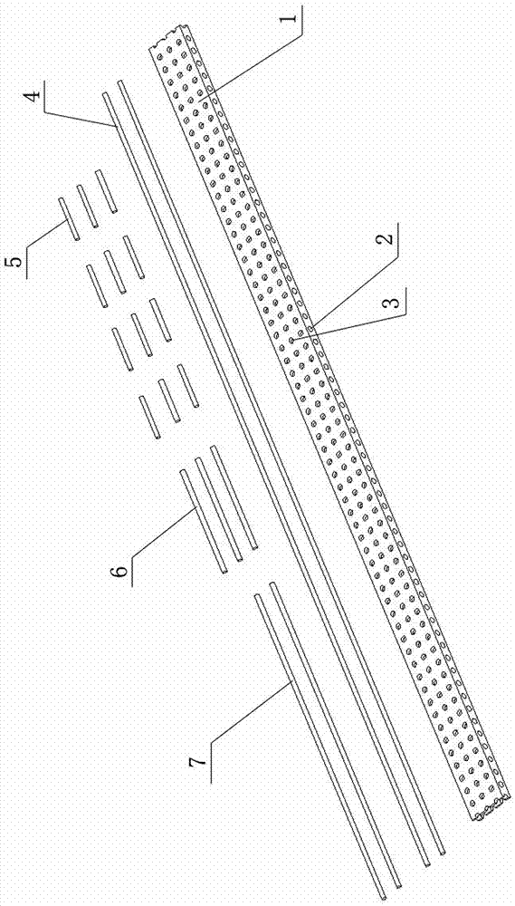
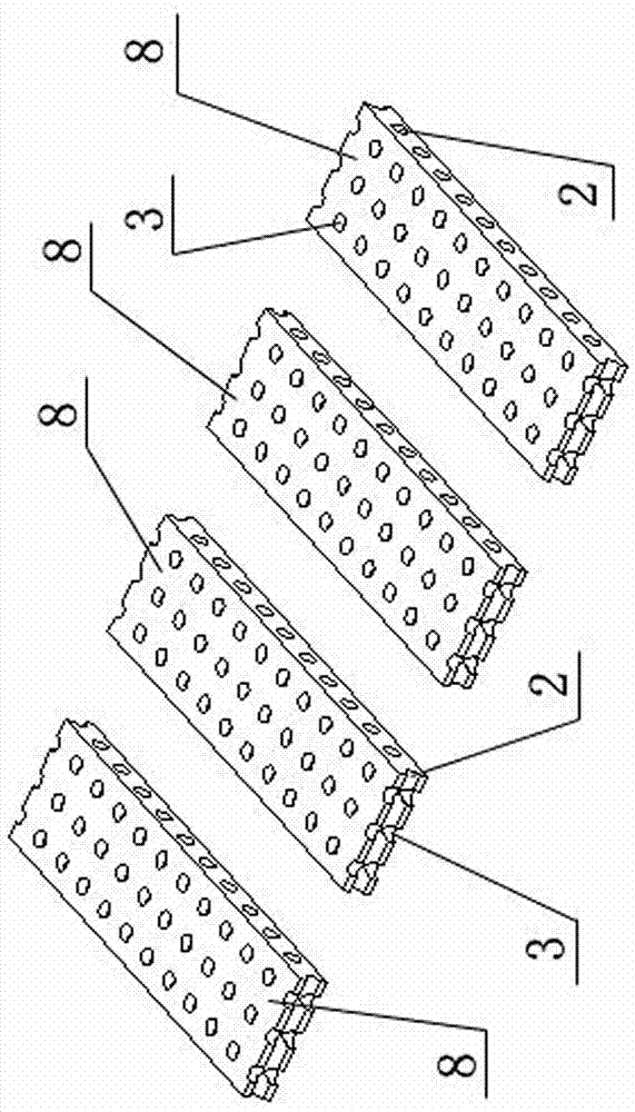
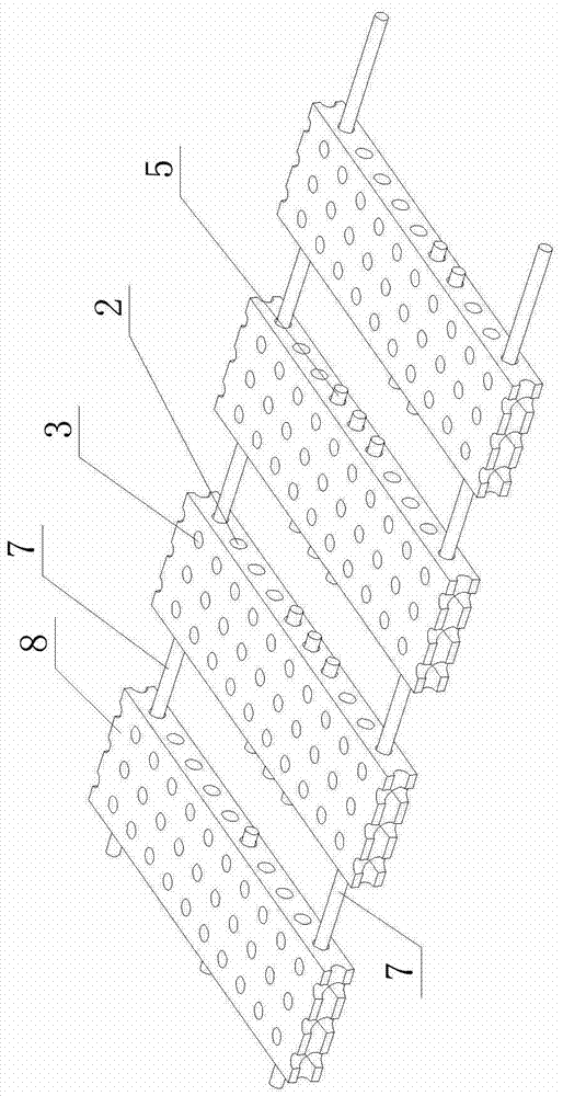
[0035] Such as figure 1 As shown, the present invention includes a rectangular resilient insulating plate with a plurality of horizontal and vertical perforations, and conductive rods that can be inserted into the horizontal perforations. There are multiple ( figure 1 Take 60 as an example) horizontal perforations that run through the original elastic insulation board, and the direction of the horizontal perforation is consistent with the width direction of the original elastic insulation board; each horizontal perforation on the original elastic insulation board is provided with a Vertical perforation, each horizontal perforation cross-connects with its corresponding vertical perforation.

[0036] The original elastic insulating board is made of insulating material with good elasticity such as silicon rubber, elastic polyvinyl chloride and the like.

[0037] Each horizontal perforation corresponds to three vertical perforations, and the three vertical perforations are evenl...


PUM

PropertyMeasurementUnit
Diameteraaaaaaaaaa
Widthaaaaaaaaaa
Thicknessaaaaaaaaaa

Abstract

The invention discloses a high frequency circuit splicing experiment board, and belongs to the technical field of circuit experiment devices. According to the invention, to address excessive capacitance of current bread boards, a high frequency circuit splicing experiment board that is characterized by easy connection and reliable usage is provided. The experiment board includes a rectangular elastic insulating panel and a plurality of electrically conductive rods. The experiment board is structured in that: a plurality horizontal piercings that penetrate the elastic insulating panel are evenly distributed in the length direction of the elastic insulated panel, the direction of the horizontal piercings and the width direction of the elastic insulating panel are consistent; the elastic insulating panel is provided with three vertical piercings that penetrate the elastic insulating panel corresponding to respective horizontal piercings, the direction of the vertical piercings and the thickness direction of the elastic insulating panel are consistent, each vertical piercing and a corresponding horizontal piercing are in intersected communication. When the experiment board is in usage,the elastic insulating panel is sheared to a plurality of segments with a proper length along the horizontal piercings based on circuit requirements, the electrically conductive rods with a proper length are inserted to the horizontal piercings that are not damaged in shearing (the diameter of each electrically conductive rod is very close to that of each horizontal piercing), and electronic element pins or bread boards are inserted to corresponding vertical piercings. The experiment board can achieve compact touch conductivity by using elastic extruding of the elastic insulating panel.

Description

technical field [0001] The invention belongs to the technical field of circuit experiment devices, in particular to a high-frequency circuit splicing experiment board. Background technique [0002] A breadboard is a tool for solderless experimentation with electronic circuits. There are many small jacks on the breadboard, and there are conductive clips in the holes. Various electronic components can be inserted or pulled out as needed, eliminating the need for soldering, saving the assembly time of the circuit, and the components can be reused, widely used For the assembly, debugging and teaching of electronic circuits. However, the facing area between the conductive clips inside the existing breadboard is relatively large, the distance between the clips is relatively close, and the number of clips is large, resulting in a large capacitance between the clips, which is not suitable for high-frequency circuit experiments. In addition, the connection relationship between the ...

Claims


Application Information

Patent Timeline
IPC IPC(8): G09B23/18
CPCG09B23/183
Inventor 陈竹郭春芳陈光
Owner 陈竹
Features
  • R&D
  • Intellectual Property
  • Life Sciences
  • Materials
  • Tech Scout
  • Unparalleled Data Quality
  • Higher Quality Content
  • 60% Fewer Hallucinations
Learn More