
Method for double-side interconnection silicon-based IGBT module employing low-temperature sintered nano-silver

A low-temperature sintering, nano-silver technology, applied in electrical components, electric solid devices, circuits, etc., can solve the problems of low connection strength, non-volatile nano-silver solder paste, low connection strength, etc., and achieve the effect of low cost

Inactive Publication Date: 2018-04-06
TIANJIN UNIV
View PDF4 Cites 11 Cited by
  • Summary
  • Abstract
  • Description
  • Claims
  • Application Information

AI Technical Summary

Problems solved by technology

However, double-sided modules using low-temperature sintered nano-silver have not been reported, mainly because the connection strength of multiple large-area chips and substrate sintering is not high (below 30 MPa), especially with bare copper DBC substrates.
Since the connection between the chip and the bare copper DBC substrate requires an oxygen-free environment, the organic matter in the nano-silver solder paste cannot be volatilized during the sintering connection process, resulting in a lower connection strength.

Method used


Image

  • Method for double-side interconnection silicon-based IGBT module employing low-temperature sintered nano-silver
  • Method for double-side interconnection silicon-based IGBT module employing low-temperature sintered nano-silver
  • Method for double-side interconnection silicon-based IGBT module employing low-temperature sintered nano-silver

Examples


Embodiment Construction

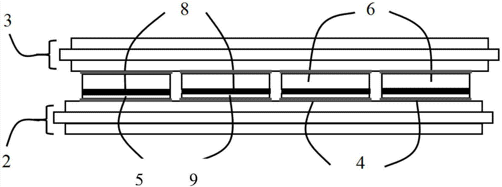
[0027] The specific implementation manner of the present invention will be described in detail below in conjunction with the accompanying drawings.

[0028] The method for double-sided interconnected silicon-based IGBT modules using low-temperature sintered nano-silver specifically includes the following steps:

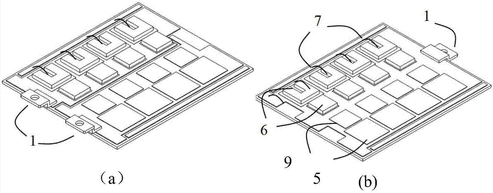
[0029] Step 1, using ultrasonic welding technology to realize the connection between the terminal 1 of the double-sided interconnected silicon-based IGBT module and the electrode area of ​​the DBC substrate. The material of the terminal and the electrode area of ​​the DBC substrate is pure copper. Ultrasonic welding power is 1.3-1.6W.

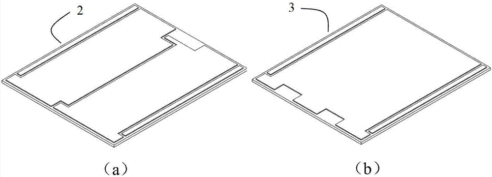
[0030] Step 2: The material of the DBC substrate is selected as a bare copper ceramic plate, which has high thermal conductivity and thermal expansion coefficient. Such as figure 2 As shown, 2 is the upper DBC substrate, and 3 is the lower DBC substrate. The impurities on the surface of the upper DBC substrate 2 and the lower DBC ...


PUM


Abstract

The invention relates to a method for a double-side interconnection silicon-based IGBT module employing low-temperature sintered nano-silver, and the module consists of a power terminal, an upper DBCsubstrate, a lower DBC substrate, a nano-silver soldering paste, a silicon-based IGBT chip, a buffering layer, a thick aluminum wire, a soldering lug, a silicon-based diode chip, silica gel and moldedresin. The lower surface of the silicon-based IGBT chip, the lower surface of the silicon-based diode chip and the lower surface of the buffering layer are connected with the lower DBC substrate through nano-silver. Meanwhile, the upper surface of the silicon-based IGBT chip, the upper surface of the silicon-based diode chip and the upper surface of the buffering layer are connected with the upper DBC substrate through nano-silver. The connection strength of the chip and the buffering layer with the DBC substrates can reach 30MPa. The silicon-based IGBT chip and the silicon-based diode chip of the lower DBC substrate and the upper surface of the buffering layer are connected with the buffering layer of the upper DBC substrate and the upper surfaces of the silicon-based IGBT chip and the silicon-based diode chip through an SnAgCu soldering lug or an SnAg soldering lug, thereby obtaining the double-side interconnection silicon-based IGBT module.

Description

technical field [0001] The invention relates to the field of power semiconductor packaging and power modules, in particular to a double-sided interconnected silicon-based IGBT module packaged with low-temperature sintered nano-silver. Background technique [0002] With the development of power electronics technology, high-power conversion system devices (such as silicon-based IGBT modules) have attracted more and more attention. At the same time, the need for energy saving and low cost also urgently requires the high-power silicon-based IGBT module to be lighter and smaller. However, this demand has brought great challenges to the development of high-power silicon-based IGBT modules, because light weight and miniaturization will lead to an increase in the current density of the module, which will cause higher heat to be generated inside the module, causing junction temperature rise. If the generated heat cannot be discharged in time, the high junction temperature will affe...

Claims


Application Information

Patent Timeline
IPC IPC(8): H01L25/07H01L25/18H01L23/488H01L21/60
CPCH01L24/31H01L24/83H01L25/072H01L25/18H01L25/50H01L2224/32501H01L2224/335H01L2224/8384H01L2924/01047H01L2224/32225H01L2224/33
Inventor 梅云辉刘文付善灿陆国权李欣
Owner TIANJIN UNIV
Learn More