A through-silicon via test structure and test method thereof

A technology of test structure and test method, applied in semiconductor/solid-state device testing/measurement, semiconductor/solid-state device components, semiconductor devices, etc., can solve the problems of high test cost, failure, complex test structure, etc., and achieve simple and convenient testing. , the effect of simple structure

Active Publication Date: 2020-08-18
SEMICON MFG INT (SHANGHAI) CORP +1
View PDF6 Cites 0 Cited by
  • Summary
  • Abstract
  • Description
  • Claims
  • Application Information

AI Technical Summary

Problems solved by technology

There is a method for measuring the depth of TSVs in the current technology, but the method needs to form a microfluidic pressure sensing device on the surface of TSVs for detection, the test structure is relatively complicated, the detection is cumbersome, and the test cost is high
[0005] There are other TSV test structures in the current process, which can judge whether the insulating layer is complete by measuring whether there is leakage current, or judge whether the depth of the TSV reaches the standard value by measuring the capacitance value, but in the above In the structure and test method, the test total capacitance Ct includes oxide capacitance and depletion capacitance, so the test total capacitance Ct is smaller than the oxide capacitance, so that the test sensitivity is not accurate enough
Furthermore, for the leakage current test, if there are defects in the depletion layer, the leakage current will also be blocked, so that the leakage current test sensitivity is reduced or invalid

Method used


Image

  • A through-silicon via test structure and test method thereof
  • A through-silicon via test structure and test method thereof
  • A through-silicon via test structure and test method thereof

Examples


Embodiment 1

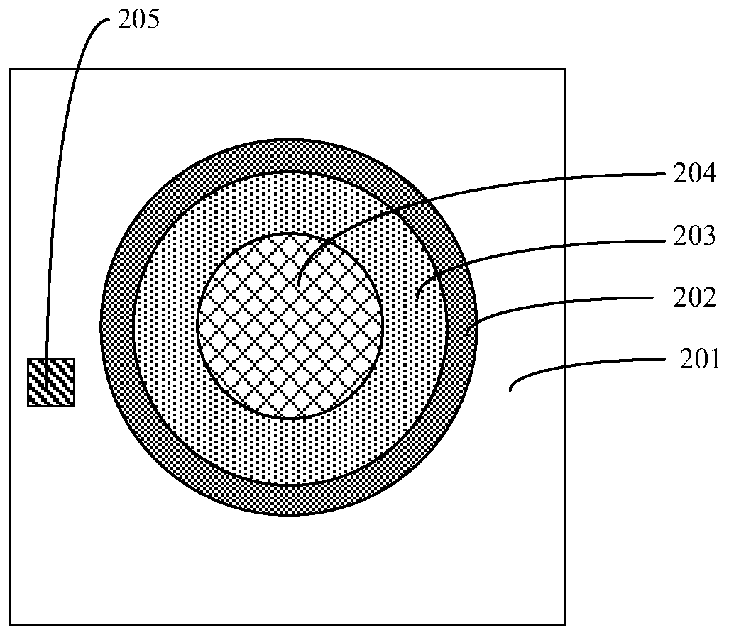
[0074] In order to make the objects, features and advantages of the present invention more comprehensible, specific implementations of the present invention will be described in detail below in conjunction with the accompanying drawings. in, Figure 3A-Figure 3Bis a schematic structural view of a TSV test structure according to an embodiment of the present invention; Figure 3A A top view of the TSV test structure; Figure 3A is a cross-sectional view of the TSV test structure.

[0075] In the following description, specific details are set forth in order to provide a thorough understanding of the present invention. However, the present invention can be implemented in many other ways than those described here, and those skilled in the art can make similar extensions without departing from the connotation of the present invention. Accordingly, the invention is not limited to the specific implementations disclosed below.

[0076] Embodiments of the present invention firstly ...

Embodiment 2

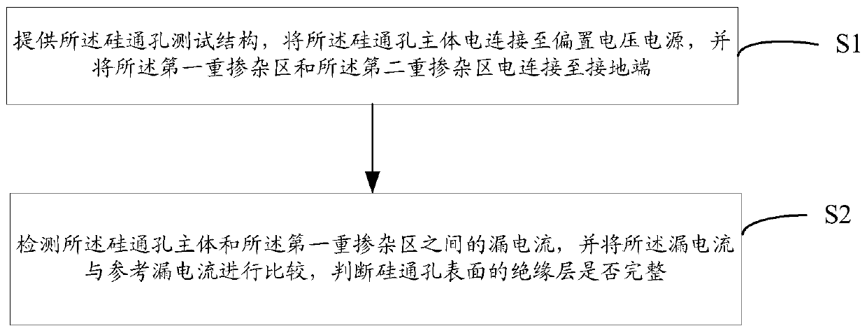
[0116] The embodiment of the present invention also provides a test method for testing the integrity of the insulating layer on the surface of the TSV using the TSV test structure, please refer to figure 1, is a schematic flow chart of the test method, specifically including:

[0117] providing the TSV test structure, electrically connecting the TSV main body to a bias voltage power supply, and electrically connecting the first heavily doped region and the second heavily doped region to a ground terminal;

[0118] Detecting the leakage current between the main body of the TSV and the first heavily doped region, and comparing the leakage current with a reference leakage current to determine whether the insulating layer on the surface of the TSV is complete.

[0119] Wherein, when the detected leakage current is greater than the reference leakage current, the thickness of the insulating layer is uneven, the insulating performance of the insulating layer does not meet the require...

Embodiment 3

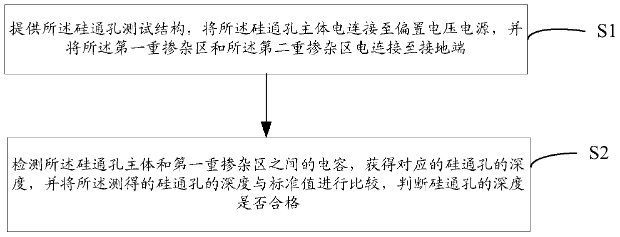
[0125] The embodiment of the present invention also provides a test method for testing whether the depth of the TSV is qualified by using the TSV test structure, please refer to figure 2 , is a schematic flow chart of the test method, specifically including:

[0126] providing the TSV test structure, electrically connecting the TSV main body to a bias voltage power supply, and electrically connecting the first heavily doped region and the second heavily doped region to a ground terminal;

[0127] Detecting the capacitance between the main body of the TSV and the first heavily doped region, obtaining the depth of the corresponding TSV, and comparing the measured depth of the TSV with a standard value to determine the TSV Whether the depth is qualified.

[0128] Optionally, the capacitance between the TSV main body and the first heavily doped region is linear and positively correlated with the TSV depth, and when the TSV main body and the first heavily doped region are detecte...


PUM

PropertyMeasurementUnit
thicknessaaaaaaaaaa
thicknessaaaaaaaaaa

Abstract

The invention provides a silicon through hole testing structure and method, and the structure comprises a semiconductor substrate which is of a first conductive type; a silicon through hole which is located in the semiconductor substrate and comprises a through hole main body and an insulating layer from the inside to the outside; a first heavy doped region which is of a second conductive type, islocated in the semiconductor substrate and is set around the silicon through hole; a second heavy doped region which is of a first conductive type, is located in the semiconductor substrate and is set outside the first heavy doped region at intervals; and an interconnection structure which is electrically connected with the silicon through hole, the first heavy doped region and the second heavy doped region. The structure can measure whether there is a leaked current or not to judge whether an insulating layer is complete or not, and also can measure a capacitance value to judge whether the depth of the silicon through hole reaches a standard value or not. Moreover, the leaked current and the capacitance value are more accurate and sensitive, thereby achieving the more accurate testing ofwhether the insulating layer is complete or not and whether the depth of the silicon through hole reaches the standard value or not.

Description

technical field [0001] The invention relates to the technical field of semiconductors, in particular to a through-silicon via test structure and a test method thereof. Background technique [0002] With the continuous development of semiconductor technology, the feature size of semiconductor devices has become very small. It is becoming more and more difficult to increase the number of semiconductor devices in a two-dimensional packaging structure. Therefore, three-dimensional packaging has become a method that can effectively improve chip integration. degree method. Current three-dimensional packaging includes die stacking based on gold wire bonding, package stacking and three-dimensional stacking based on through silicon vias (Through Silicon Via, TSV). Among them, the three-dimensional stacking technology using through-silicon vias has the following three advantages: (1) high-density integration; (2) greatly shortening the length of electrical interconnections, which can...

Claims


Application Information

Patent Timeline
Patent Type & Authority Patents(China)
IPC IPC(8): H01L21/66H01L23/544
CPCH01L22/14H01L22/34
Inventor 甘正浩邵芳
Owner SEMICON MFG INT (SHANGHAI) CORP
Why Eureka
Try Eureka