Memory structure and method of forming the same

A memory and storage layer technology, which is applied in the manufacturing of semiconductor devices, electric solid state devices, and semiconductor/solid state devices, etc., can solve the problems of increasing process difficulty, circuit breakage, and process cost increase, and achieves the goal of reducing process difficulty, improving performance, and saving Process cost effect

Active Publication Date: 2021-11-12
YANGTZE MEMORY TECH CO LTD
View PDF4 Cites 0 Cited by
  • Summary
  • Abstract
  • Description
  • Claims
  • Application Information

AI Technical Summary

Problems solved by technology

However, due to the need to open the insulating layer and the wafer to form through-wafer vias at the same time for circuit connection, the increase in the thickness of the insulating layer will lead to an increase in the aspect ratio of the through-wafer vias, and it is also necessary to strictly control the feature size and shape of the through-wafer vias. In appearance, the deviation of the process may lead to circuit breakage or leakage, which greatly increases the difficulty of the process, requires more advanced semiconductor processing machines, and increases the cost of the process.

Method used


Image

  • Memory structure and method of forming the same
  • Memory structure and method of forming the same
  • Memory structure and method of forming the same

Examples


Embodiment Construction

[0031] The specific implementation of the memory structure and its forming method provided by the present invention will be described in detail below in conjunction with the accompanying drawings.

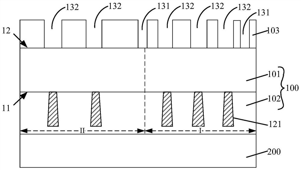
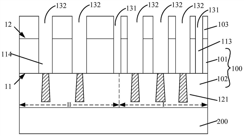
[0032] Please refer to Figure 1 to Figure 7 , is a structural schematic diagram of the forming process of the memory structure according to a specific embodiment of the present invention.

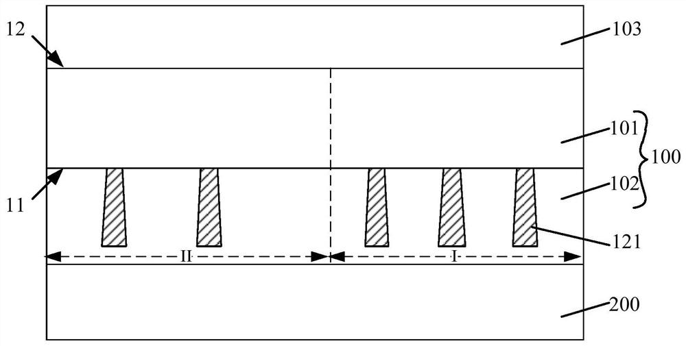
[0033] Please refer to figure 1 , providing a first substrate 100, comprising: a substrate layer 101 and a storage layer 102, the substrate layer 101 has a first surface 11 and a second surface 12 opposite to each other, and the storage layer 102 is located on the first surface of the substrate layer 101 11 , the first substrate 100 includes a pad region I; a dielectric layer 103 is formed on the second surface 12 of the substrate layer 101 .

[0034] figure 1 In this case, the first substrate 100 is in an upside-down state, at this time, the first surface 11 of the substrate layer 101 is t...


PUM

PropertyMeasurementUnit
thicknessaaaaaaaaaa
thicknessaaaaaaaaaa
thicknessaaaaaaaaaa

Abstract

The present invention relates to a memory structure and a forming method thereof. The memory structure includes: a first base, including: a substrate layer and a storage layer, the substrate layer has a first surface and a second surface opposite to each other, and the storage layer is located on On the first surface of the substrate layer, the first substrate includes a pad area; a dielectric layer located on the second surface of the substrate layer; a solder pad located on the surface of the dielectric layer on the pad area; isolation The structure penetrates through the substrate layer, is located at the edge of the pad region, surrounds the substrate layer in the pad region, and is used to isolate the substrate layer in the pad region from the substrate layer around the isolation structure. In the memory structure of the present invention, the parasitic capacitance between the pad and the substrate layer is reduced, which is beneficial to improving memory performance.

Description

technical field [0001] The invention relates to the field of semiconductor technology, in particular to a memory structure and a forming method thereof. Background technique [0002] In recent years, the development of flash memory (Flash Memory) is particularly rapid. The main feature of flash memory is that it can keep stored information for a long time without power on, and has the advantages of high integration, fast access speed, easy erasing and rewriting, etc. Has been widely used. In order to further increase the bit density (Bit Density) of the flash memory while reducing the bit cost (Bit Cost), three-dimensional flash memory (3D NAND) technology has been developed rapidly. [0003] The 3D NAND flash memory structure includes a storage array structure and a CMOS circuit structure above the storage array structure. The storage array structure and the CMOS circuit structure are usually formed on two different wafers, and then bonded to The CMOS circuit wafer is bo...

Claims


Application Information

Patent Timeline
Patent Type & Authority Patents(China)
IPC IPC(8): H01L27/11524H01L27/11551H01L27/1157H01L27/11578
CPCH01L29/0649H01L21/76224H10B41/35H10B41/27H10B43/35H10B43/27H01L2224/05624H01L2224/05639H01L2224/05644H01L2224/05647H01L2224/05553H01L2224/05096H01L24/05H01L2224/0557H01L2924/00014H01L2924/30105H01L21/76202H01L21/76877H01L21/31116H10B41/41H10B41/42H10B43/20
Inventor 陈赫董金文朱继锋华子群肖亮王永庆
Owner YANGTZE MEMORY TECH CO LTD
Why Eureka
Try Eureka