Uniform light element for DMD digital photolithography system and design method thereof

A lithography system and design method technology, applied in the field of digital lithography, can solve the problems of backward development of lithography data processing software for high-speed drive boards, lack of efficient light uniform components, and influence on light uniformity effects, etc., to achieve light energy reflection and Less refraction loss, improved uniform light effect, improved uniformity of light intensity

Inactive Publication Date: 2018-04-20
NORTHEAST NORMAL UNIVERSITY
View PDF4 Cites 12 Cited by
  • Summary
  • Abstract
  • Description
  • Claims
  • Application Information

AI Technical Summary

Problems solved by technology

However, domestic DMD digital lithography technology is still relatively backward and develops slowly
There are two main reasons: one is that the development of DMD's high-speed driver board and the corresponding lithography data processing software is backward
Second, there is a lack of efficient uniform light components
At present, the commonly used dodging method is to use the traditional microlens array or the abdominal microlens array as the dodging element. This method has a good dodging effect and high energy utilization rate, but its structure is complex, it occupies a large volume, and it is not conducive to integration. Moreover, since the light source in the lithography system is mostly a coherent light source, and its sub-lenses are arranged periodically, there will be coherent fringes on the target surface, which will affect the uniform light effect

Method used


Image

  • Uniform light element for DMD digital photolithography system and design method thereof
  • Uniform light element for DMD digital photolithography system and design method thereof
  • Uniform light element for DMD digital photolithography system and design method thereof

Examples


Embodiment Construction

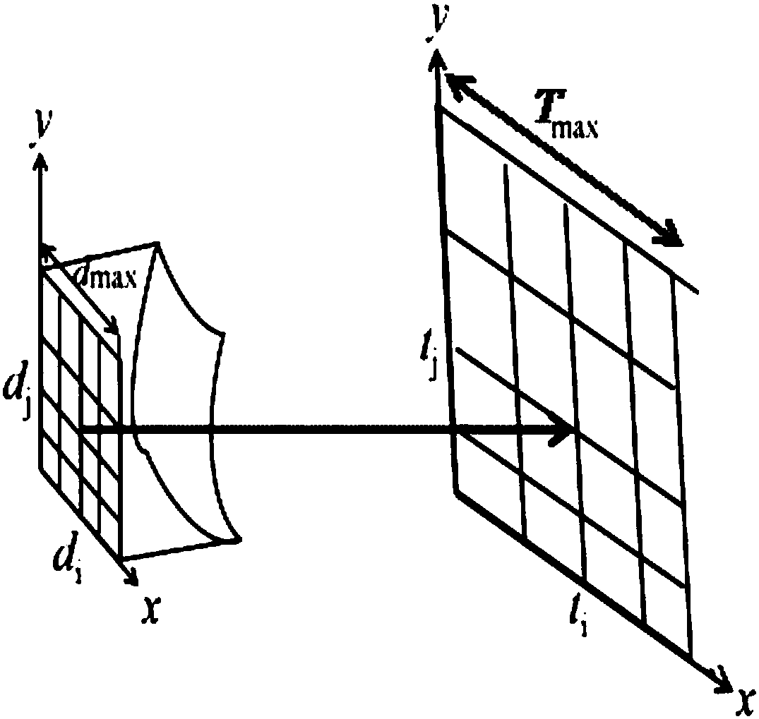
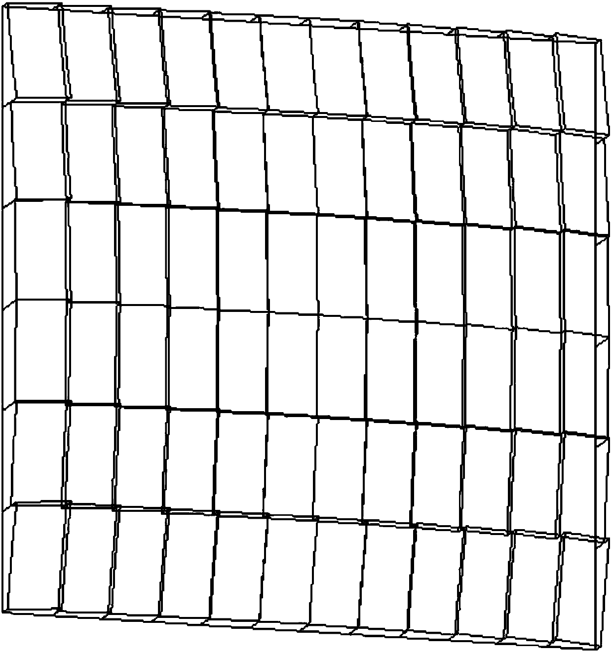
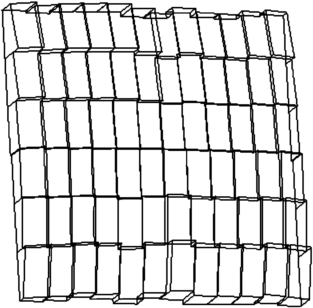
[0029] According to the non-imaging optical design theory, the free-form surface of the rear surface of the sub-lens is designed. Using the principle of energy mapping, calculate the relative position of each sub-lens and the shape of the free-form surface on the rear surface, and process on a whole piece of lens material, only the rear surface of the material is processed to form "sub-lenses" one by one, and complete the "sub-lens" of the sub-lens Stitching" to design a complete free-form surface microlens array.

[0030] Such as figure 1 As shown in Fig. 1, the free-form surface and the target surface are first divided into equal-energy grids, and then the one-to-one correspondence between the free-form surface and the target surface is established according to the method of energy mapping. The present invention is mainly applied to DMDs with an aspect ratio of 1:2, so the aspect ratio of each sub-lens is also designed to be 1:2. Taking the front surface of the sub-lens as...


PUM


Abstract

The present invention provides a uniform light element for a DMD digital photolithography system and a design method thereof, belonging to the field of digital photolithography technology. The methodcomprises more than one sub lens, each sub lens is one square with a length-width ratio of 1:2, the front surface of each sub lens is a plane, and the rear surface of each sub lens is a free curved surface. The uniform light element for the DMD digital photolithography system and the design method thereof are high in utilization rate of luminous energy, good in uniform light effect, small in sizeand convenient to integrate, can perform individual design of each sub lens, employ a mode of random arrangement of area sizes and positions, break periodicity of a traditional microlens array and greatly improve the uniform light effect of a coherent source.

Description

technical field [0001] The invention belongs to the technical field of digital lithography, and in particular relates to a uniform light element for realizing a coherent point light source. Background technique [0002] With the rapid development of the circuit board, flat panel display and digital printing industries, these industries have higher and higher requirements for the photolithography exposure technology necessary in the production process, and the photolithography exposure technology has become a factor that restricts its integration and efficiency. As a key factor, it can be said that lithography exposure technology and the development of these industries complement each other and are inseparable. Lithography exposure technology has gone through the process from proximity or contact exposure to step projection exposure and then to scanning projection exposure, but without exception, these technologies all use masks as image sources. With the continuous developm...

Claims


Application Information

Patent Timeline
Patent Type & Authority Applications(China)
IPC IPC(8): G02B27/09G03F7/20
CPCG02B27/0927G02B27/0961G03F7/2057
Inventor 刘华刘中元李乾坤李金环
Owner NORTHEAST NORMAL UNIVERSITY
Why Eureka
Try Eureka