Shifting register unit and driving method thereof as well as gate drive circuit and display device

A shift register, unit group technology, applied in static memory, digital memory information, instruments, etc., can solve the problems of poor stability, high power consumption, and short working life of GOA circuits

Pending Publication Date: 2018-04-20
BOE TECH GRP CO LTD +1
View PDF5 Cites 17 Cited by
  • Summary
  • Abstract
  • Description
  • Claims
  • Application Information

AI Technical Summary

Problems solved by technology

[0004] Embodiments of the present invention provide a shift register unit and its driving method, a gate driving circuit and a display devic...

Method used


Image

  • Shifting register unit and driving method thereof as well as gate drive circuit and display device
  • Shifting register unit and driving method thereof as well as gate drive circuit and display device
  • Shifting register unit and driving method thereof as well as gate drive circuit and display device

Examples


Embodiment 1

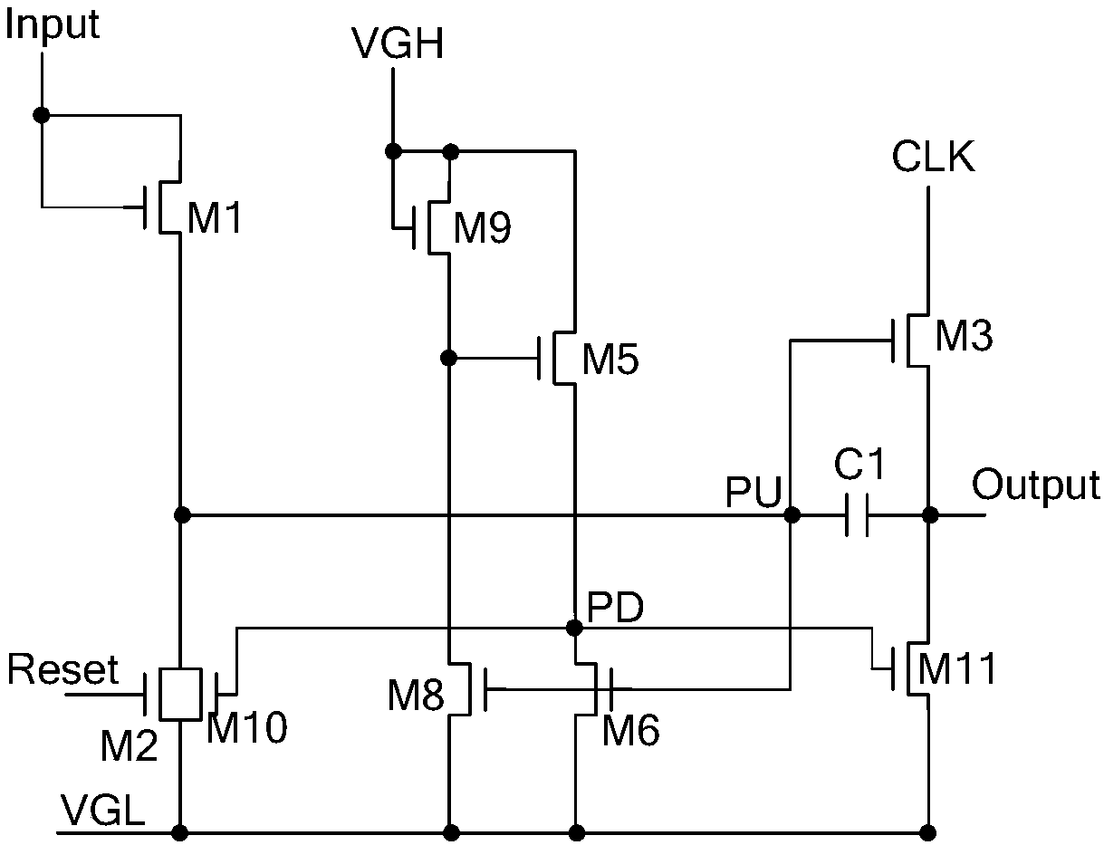
[0058] An embodiment of the present invention provides a shift register unit, such as Figure 6 As shown, it includes: a pull-up control module 10 , a pull-up module 20 , a pull-down control module 30 , a pull-down module 40 , a reset module 60 , and a denoising module 50 , that is, M=1.

[0059] Wherein, the pull-up control module 10 is connected to the signal input terminal Input and the pull-up node PU, and the pull-up control module 10 is used to pull up the potential of the pull-up node PU to the signal input terminal Input under the control of the signal input terminal Input.

[0060] The pull-up module 20 is connected to the pull-up node PU, the clock signal terminal CLK and the signal output terminal Output. The pull-up module 20 is used to output the signal of the clock signal terminal CLK to the signal output terminal Output under the control of the pull-up node PU.

[0061] The pull-down control module 30 is connected to the first control terminal Ctr, the pull-down...

Embodiment 2

[0095] Embodiments of the present invention provide a Figure 10 The shift register unit shown is different from the first embodiment in that the shift register unit includes a denoising module 50 and a denoising module 50', that is, M=2. The denoising module 50' is connected to the second control terminal TRSTb, the pull-up node PU, the signal output terminal Output and the first voltage terminal VGL, and the denoising module 50' is used to control the pull-up node PU under the control of the second control terminal TRSTb The potential of the sum signal output terminal Output is pulled down to the first voltage terminal VGL.

[0096] On this basis, the circuit structure of the denoising module 50' can be as follows Figure 11 It includes the twelfth transistor M12 and the thirteenth transistor M13, the connection relationship of which is the same as the structure of the denoising module 50 in the first embodiment, which will not be repeated in the present invention.

[0097...

Embodiment 3

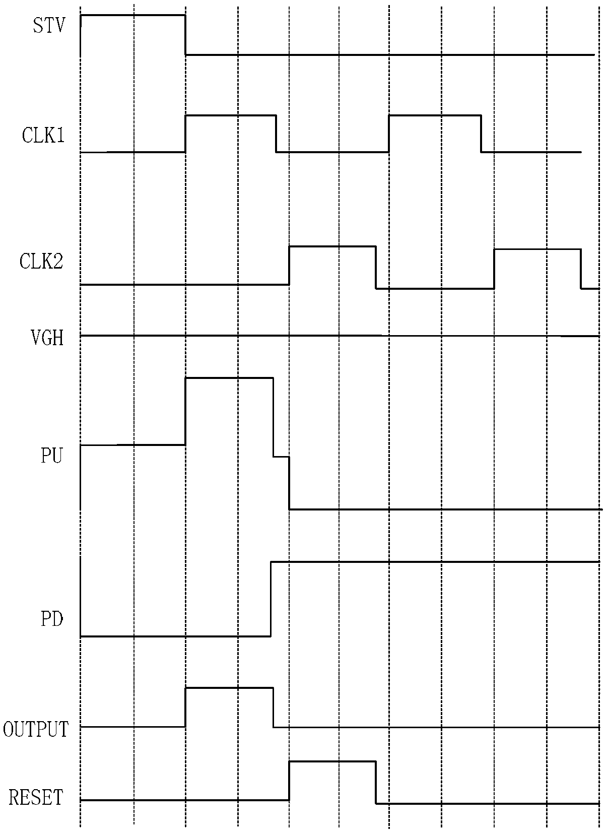
[0106] An embodiment of the present invention provides a driving method for a shift register unit as described in Embodiment 1. Refer to Figure 9a and Figure 9b As shown, in an image frame, the driving method includes:

[0107] Input stage P1: Input=1, CLK=CLK1=0, Ctr=1, TRSTa=0, PU=1, PD=0, Output=0.

[0108] The pull-up control module 10 pulls up the potential of the pull-up node PU to the signal input terminal Input under the control of the signal input terminal Input; the pull-down control module 30 pulls the potential of the pull-up node PU and the first control terminal Ctr under the control of the pull-up node PU The potential of the node PD is pulled down to the first voltage terminal VGL.

[0109] Specifically, since the signal input terminal Input is at a high level, under the control of the signal input terminal Input, the first transistor M1 is turned on, and the high level of the signal input terminal Input is output to the pull-up node PU through the first tr...


PUM


Abstract

The embodiments of the invention provide a shifting register unit and a driving method thereof as well as a gate drive circuit and a display device, and relates to the technical field of display, aiming at solving the problems of poor stability, short working life and high power consumption of the existing (gate driver on array) GOA circuit at the same time. The shifting register unit comprises apull-up control module, a pull-up module, a pull-down control module, a pull-down module, a reset module and M de-noising modules, wherein the de-noising modules are connected with a second control terminal, a pull-up node, a signal output end and a first voltage terminal, and are used for pulling the electric potentials of the pull-up node and the signal output end down to the first voltage terminal under the control of the second control terminal. The shifting register unit is used for outputting gate line scanning signals for a gate line connected with the shifting register unit.

Description

technical field [0001] The present invention relates to the field of display technology, in particular to a shift register unit, a driving method thereof, a gate driving circuit and a display device. Background technique [0002] In TFT-LCD (Thin Film Transistor Liquid Crystal Display, thin film transistor-liquid crystal display) technology, in order to achieve low cost and narrow frame, GOA (English full name: Gate driver On Array, Chinese name: gate driver circuit integrated on the substrate The above) technology, that is, the gate drive circuit is integrated inside the panel through the thin film transistor process, so as to realize the advantages of narrow frame and reduce IC (full name in English: Integrated Circuit, Chinese name: integrated circuit) and assembly cost. [0003] When designing the GOA circuit, it is necessary to focus on the gate bias time of each thin film transistor in the GOA circuit, so as to prevent the excessive threshold voltage shift (Vth shift) ...

Claims


Application Information

Patent Timeline
IPC IPC(8): G09G3/36G11C19/28
CPCG09G3/3696G11C19/28G09G2310/0286G09G2310/0267G09G3/20G11C19/287G09G2310/08G09G3/3677
Inventor 张元波王孝林许卓陈帅刘珠林
Owner BOE TECH GRP CO LTD
Why Eureka
Try Eureka