Flash memory unit structure with high coupling ratio and preparation method thereof

A flash memory cell, high coupling technology, used in electrical components, semiconductor/solid state device manufacturing, transistors, etc., can solve the problems of increasing the flash memory cell coupling rate, reducing the effective width of the tunnel oxide layer, etc., to improve erasing efficiency, improve Flash memory performance, the effect of improving the coupling rate

Inactive Publication Date: 2018-04-20
SHANGHAI HUALI MICROELECTRONICS CORP
View PDF4 Cites 8 Cited by
  • Summary
  • Abstract
  • Description
  • Claims
  • Application Information

AI Technical Summary

Problems solved by technology

Reducing the effective width of the tunnel oxide layer can increase the coupling rate of the flash memory cell, but there is no public report on the structure of the flash memory cell and its preparation method.

Method used


Image

  • Flash memory unit structure with high coupling ratio and preparation method thereof
  • Flash memory unit structure with high coupling ratio and preparation method thereof
  • Flash memory unit structure with high coupling ratio and preparation method thereof

Examples


Embodiment Construction

[0039] The following will clearly and completely describe the technical solutions in the embodiments of the present invention with reference to the accompanying drawings in the embodiments of the present invention. Obviously, the described embodiments are only some, not all, embodiments of the present invention. Based on the embodiments of the present invention, all other embodiments obtained by persons of ordinary skill in the art without creative efforts fall within the protection scope of the present invention.

[0040] It should be noted that, in the case of no conflict, the embodiments of the present invention and the features in the embodiments can be combined with each other.

[0041] The present invention will be further described below in conjunction with the accompanying drawings and specific embodiments, but not as a limitation of the present invention.

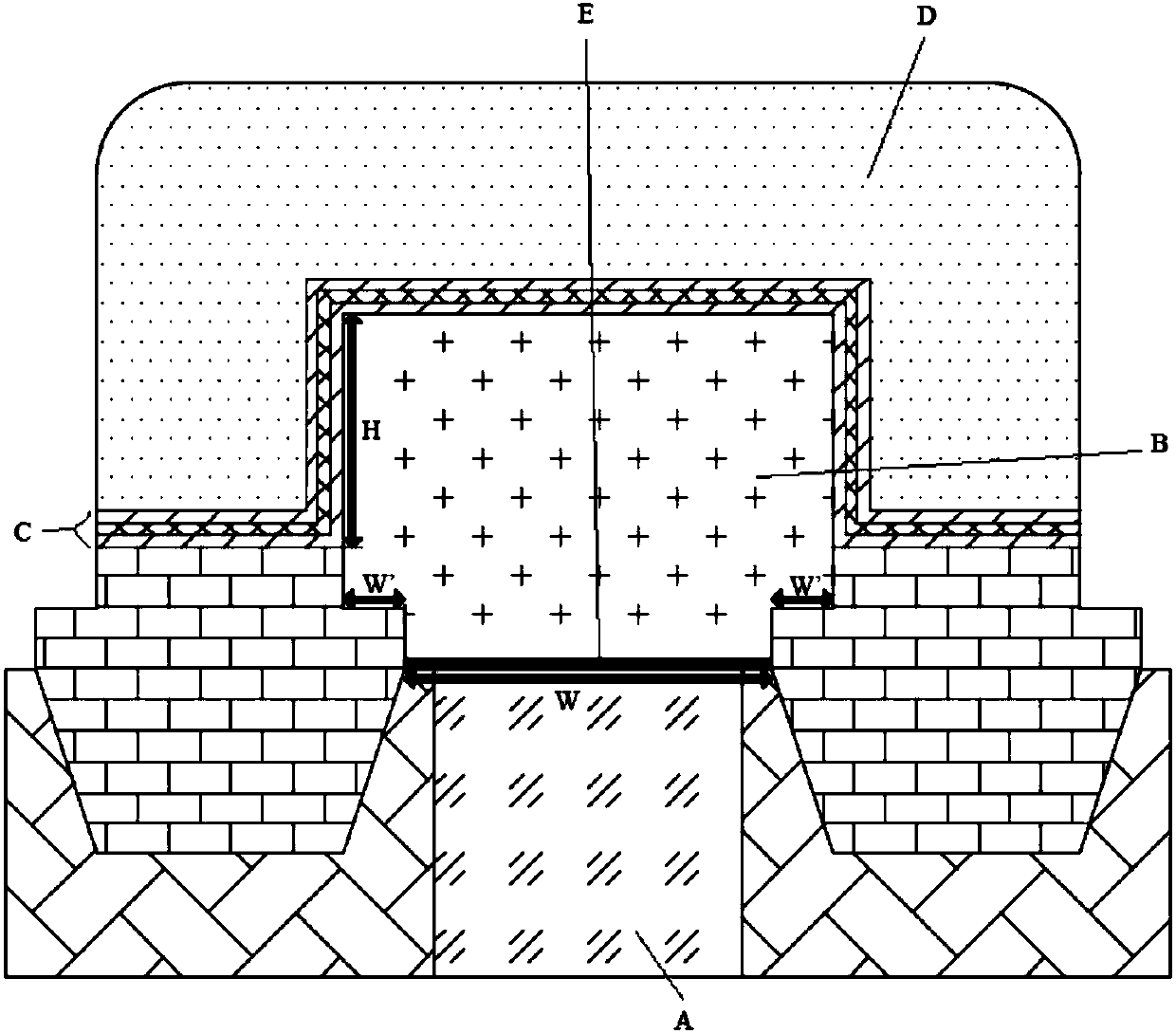
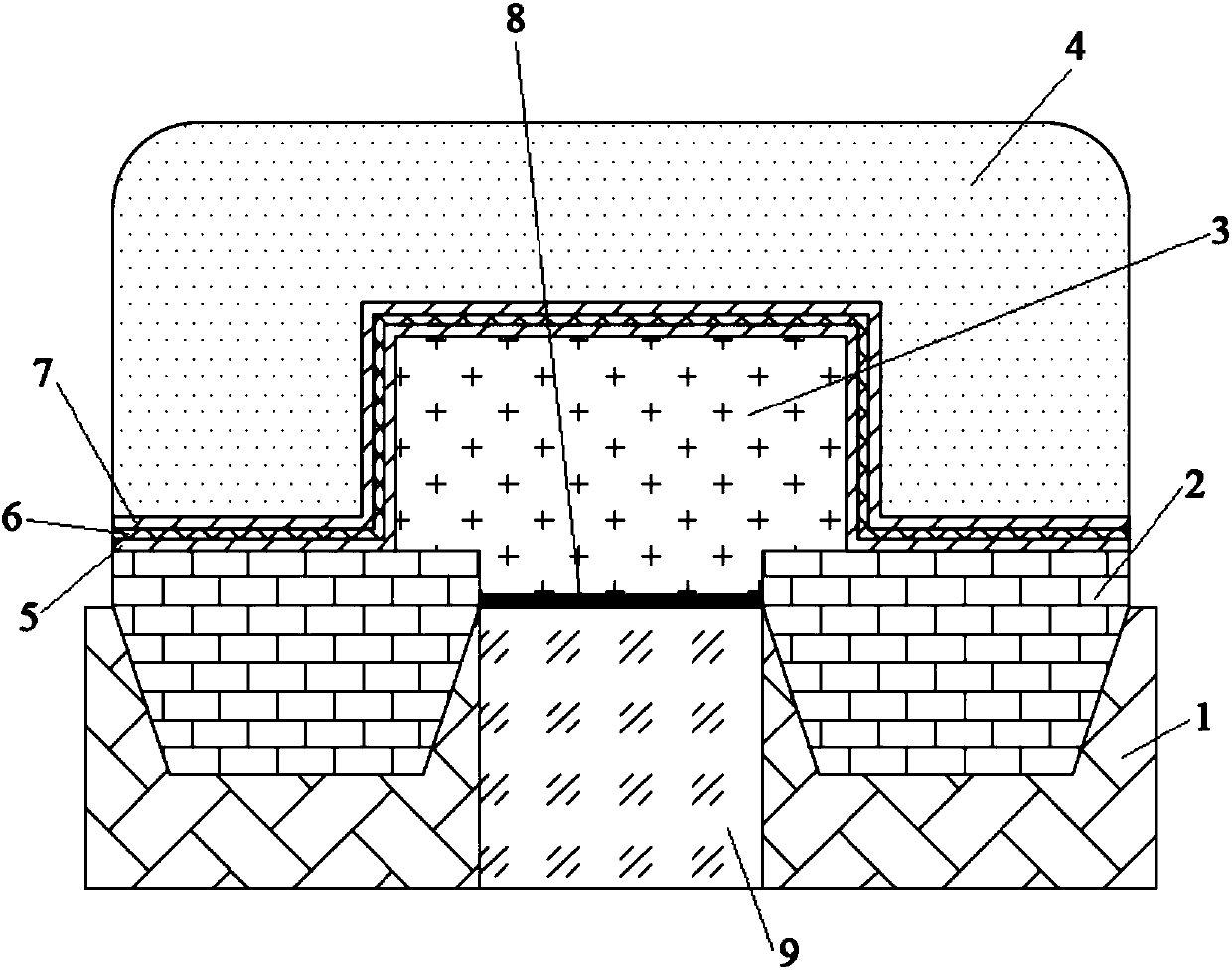
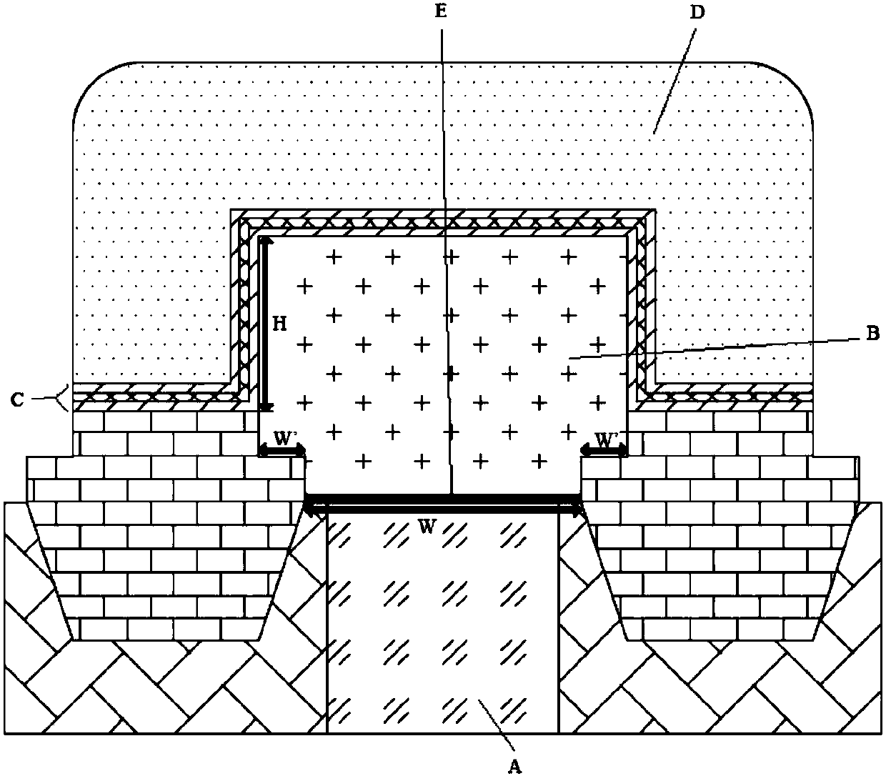
[0042] For a flash memory cell, a commonly used erasing method is to use Fowler-Nordheim tunneling (Fowler-Nordh...


PUM


Abstract

The present invention relates to a flash memory unit structure with a high coupling ratio and a preparation method thereof. The flash memory unit structure comprises: a semiconductor substrate, wherein the semiconductor substrate comprises two shallow trench isolations and an active area, and the active area is located in the semiconductor substrate between the two shallow trench isolations; a tunneling oxide layer; a floating gate; a dielectric layer; and a control gate, wherein the dimensions of the top portions of the two shallow trench isolations are equal to the dimension of the top portion of the active area, and the dimension of the tunneling oxide layer is equal to the dimension of the top portion of the active area. A silicon nitride reduction resistance amount prior to depositionof the shallow trench isolations is increased to increase the dimensions of the top portions of the shallow trench isolations; and moreover, in the subsequent technology process, the top portions ofthe shallow trench isolations can be consumed, the dimensions of the top portions of the shallow trench isolations after consumption are equal to the actual dimension of the top portion of the activearea to allow the width of the bottom portion of the floating gate to be equal to the dimension of the top portion of the active layer when a subsequent floating gate process is performed so as to reduce the capacitance of the floating gate to the substrate and increase the coupling ratio of a flash unit.

Description

technical field [0001] The invention relates to the field of semiconductor technology, in particular to a structure and a preparation method of a flash memory unit with a high coupling rate. Background technique [0002] Flash memory has been widely used as the best choice for non-volatile memory applications due to its advantages such as high density, low price, electrical changeability, and erasability. At present, flash memory cells are mainly implemented at the 65nm technology node. With the demand for high-capacity flash memory, the number of chips per silicon wafer will decrease with existing technology nodes. With the maturity of new technology nodes, flash memory cells are urged to be produced with high-node technologies. This means that the size of the flash memory cell needs to be reduced. Reducing the size of the flash memory cell will reduce the width of the active area and the length of the channel of the flash memory cell, thereby affecting the performance o...

Claims


Application Information

Patent Timeline
Patent Type & Authority Applications(China)
IPC IPC(8): H01L29/788H01L21/336
CPCH01L29/66825H01L29/7883
Inventor 田志钟林建
Owner SHANGHAI HUALI MICROELECTRONICS CORP
Why Eureka
Try Eureka