Photodiode structure for improving quantum efficiency of CMOS image sensor

A photodiode and image sensor technology, applied in circuits, electrical components, semiconductor devices, etc., can solve the problems of increasing residual electrons, inter-band tunneling leakage, dark current increase, etc., to increase the width of the depletion region and improve the quantum efficiency Effect

Active Publication Date: 2018-05-04
SHANGHAI INTEGRATED CIRCUIT RES & DEV CENT +1
View PDF4 Cites 3 Cited by
  • Summary
  • Abstract
  • Description
  • Claims
  • Application Information

AI Technical Summary

Problems solved by technology

There are two ways to increase the width of the depletion region. First, you can increase the voltage, but after increasing the voltage, it will introduce band-to-band tunneling (BTBT) leakage, resulting in an increase in dark current.
The second can increase the depth of the N region of the PN junction, but after increasing the depth of the N region of the PN junction, the residual electrons after reset will be increased, resulting in poor dark light response effect

Method used


Image

  • Photodiode structure for improving quantum efficiency of CMOS image sensor
  • Photodiode structure for improving quantum efficiency of CMOS image sensor
  • Photodiode structure for improving quantum efficiency of CMOS image sensor

Examples


Embodiment Construction

[0024] In order to make the purpose, technical solution and advantages of the present invention clearer, the specific implementation manners of the present invention will be further described in detail below in conjunction with the accompanying drawings.

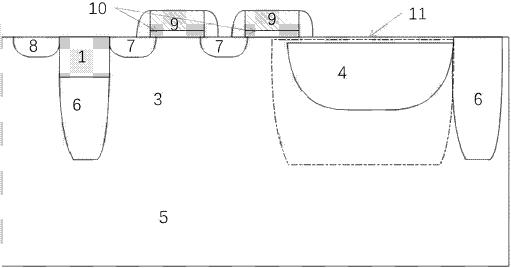
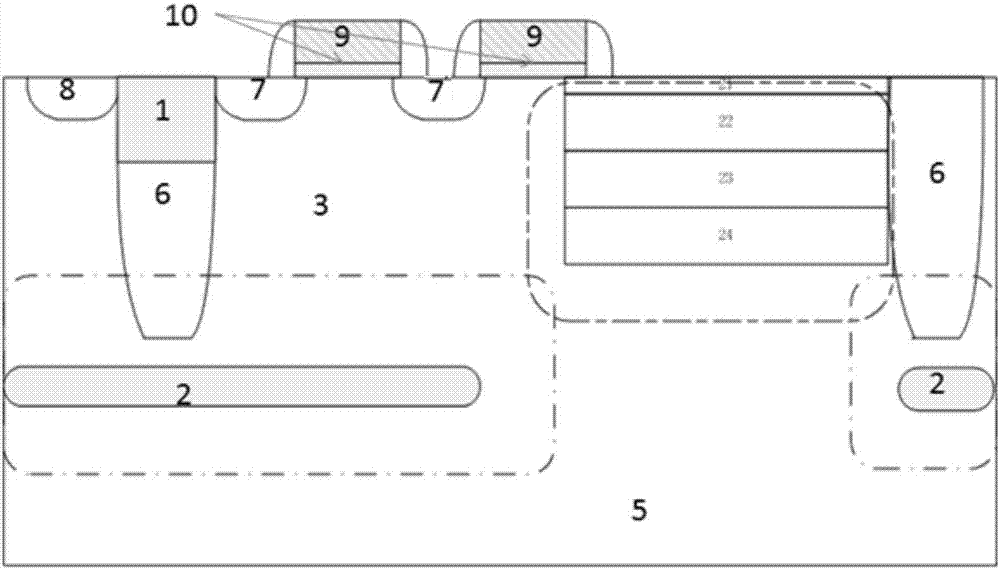
[0025] A photodiode structure for improving the quantum efficiency of a CMOS image sensor provided by the present invention is located in a lightly doped substrate, including a reset transistor, a transfer transistor, a PN photodiode, a pixel unit isolation region, a well region and a ring-shaped silicon region; The two ends of the transfer transistor are respectively connected to the reset transistor and the PN photodiode, and the well region is the well of the reset transistor; the region formed by the reset transistor, the transfer transistor and the PN photodiode is ring-shaped Surrounded by the pixel unit isolation region, the part of the pixel unit isolation region immediately adjacent to the reset transistor is shallow...


PUM


Abstract

The invention discloses a photodiode structure for improving the quantum efficiency of a CMOS image sensor. The photodiode structure is located in a lightly-doped substrate. The photodiode structure comprises a reset transistor, a transmission transistor, a PN photodiode, a pixel unit isolation region, a well region and an annular silicon region. The two ends of the transmission transistor are connected with the reset transistor and the PN photodiode respectively. A region formed by the reset transistor, the transmission transistor and the PN photodiode is surrounded by the annular pixel unitisolation region. The part of the pixel unit isolation region, adjacent to the reset transistor, is isolated from a shallow trench. The P-type region and the N-shaped region in the PN photodiode are distributed up and down in the vertical direction, and the lower part of the above space comprises a region I, a region II and a region III, wherein the three regions are different in doping concentration and are arranged from top to bottom. An annular silicon region is arranged below the well region and the pixel unit isolation region. According to the photodiode structure provided by the invention, the quantum efficiency of a long-wave section can be improved, and an inter-band tunneling electric leakage is avoided.

Description

technical field [0001] The invention relates to the field of semiconductors, in particular to a photodiode structure for improving the quantum efficiency of a CMOS image sensor. Background technique [0002] The CMOS image sensor is a photoelectric conversion device. The incident photons excite the electrons in the valence band of the semiconductor to the conduction band, store them in the reverse PN junction, and then transfer them to the capacitor through a transfer MOS transistor. [0003] The PN junction is reverse biased, that is, the drain of the reset transistor is connected to a high potential, the drain of the pass transistor is suspended, the gate of the reset transistor is set to high voltage and turned on, and the gate of the pass transistor is turned on at high voltage, at this time, the PN junction in the photodiode is clamped The charges (electrons) in the N region of the clamped photodiode are extracted, and the PN junction in the clamped photodiode is placed...

Claims


Application Information

Patent Timeline
Patent Type & Authority Applications(China)
IPC IPC(8): H01L31/109
CPCH01L31/109
Inventor 孙德明
Owner SHANGHAI INTEGRATED CIRCUIT RES & DEV CENT
Why Eureka
Try Eureka