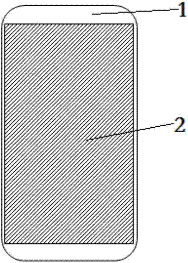
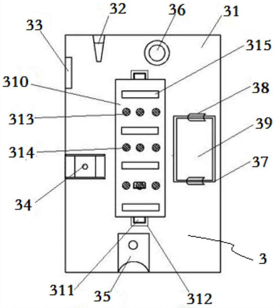
Mobile communication terminal provided with color changing OLED display screen
A technology for mobile communication terminals and display screens, which is applied in telephone communication, electrical components, circuits, etc. It can solve the problems of insufficient color of LCD display screens, affecting the status of mobile phone motherboards, and easy interference of electrical components, so as to improve installation convenience Performance and stability, wide range of color control, and improved anti-interference ability
- Summary
- Abstract
- Description
- Claims
- Application Information
AI Technical Summary
Problems solved by technology
Method used
Image
Examples
Embodiment 1
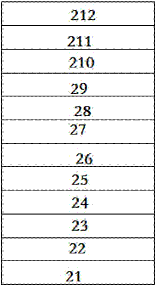
[0019] Embodiment 1: The color-changing OLED device includes a heat-dissipating adhesive layer 21, an ITO glass 22, a hole injection layer 23, a hole transport layer 24, a first light-emitting layer 25, a first energy transfer regulation layer 26, and a second layer stacked in sequence. The second light-emitting layer 27, the second energy transfer control layer 28, the third light-emitting layer 29, the electron transport layer 210, the electron injection layer 211, and the cathode electrode 212, the first and second energy transfer control layers are 9,10-two (2-naphthyl)-2-methylanthracene organic semiconductor material, the heat dissipation bonding layer is an acrylic resin layer containing alumina particles, the thickness of the heat dissipation bonding layer is 50 nanometers, and the hole injection layer It is molybdenum oxide with a thickness of 2 nanometers, the hole transport layer is TF-TCNQ with a thickness of 50 nanometers, the first and third light-emitting layers ...
Embodiment 2
[0020] Embodiment 2: The color-changing OLED device includes a heat-dissipating adhesive layer 21, an ITO glass 22, a hole injection layer 23, a hole transport layer 24, a first light-emitting layer 25, a first energy transfer regulation layer 26, and a second layer stacked in sequence. The second light-emitting layer 27, the second energy transfer control layer 28, the third light-emitting layer 29, the electron transport layer 210, the electron injection layer 211, and the cathode electrode 212, the first and second energy transfer control layers are 9,10-two (2-naphthyl)-2-methylanthracene organic semiconductor material, the heat dissipation bonding layer is an acrylic resin layer containing boron nitride particles, the thickness of the heat dissipation bonding layer is 90 nanometers, and the hole injection The layer is molybdenum oxide with a thickness of 1.5 nanometers, the hole transport layer is PEDOT-PSS with a thickness of 30 nanometers, the first and third light-emitt...
PUM
| Property | Measurement | Unit |
|---|---|---|
| thickness | aaaaa | aaaaa |
| thickness | aaaaa | aaaaa |
| band gap | aaaaa | aaaaa |
Abstract
Description
Claims
Application Information


