System-on-a-chip (SoC) production method with fault diagnosis

A system-level chip and production method technology, applied in measurement devices, instruments, measurement electronics, etc., can solve the problems of high test cost of automatic test equipment, bottlenecks in development cycle and fault location, and difficulty in improving fault coverage, so as to improve the chip The effect of testing efficiency, narrowing the scope of investigation, and saving chip area

Active Publication Date: 2018-05-08
SHANGHAI HUALI MICROELECTRONICS CORP
View PDF7 Cites 1 Cited by
  • Summary
  • Abstract
  • Description
  • Claims
  • Application Information

AI Technical Summary

Problems solved by technology

[0007] However, since multiple shift registers for fault diagnosis are set in the chip, the chip is larger in size; with the improvement of circuit integration and circuit complexity, it becomes more and more difficult to improve the fault coverage rate during fault diagnosis. The cost of testing using automatic test equipment is getting higher and higher; at the same time, the development cycle and fault location have become project bottlenecks

Method used


Image

  • System-on-a-chip (SoC) production method with fault diagnosis
  • System-on-a-chip (SoC) production method with fault diagnosis
  • System-on-a-chip (SoC) production method with fault diagnosis

Examples


Embodiment Construction

[0041] It should be noted that, in the case of no conflict, the following technical solutions and technical features can be combined with each other.

[0042] The specific embodiment of the present invention will be further described below in conjunction with accompanying drawing:

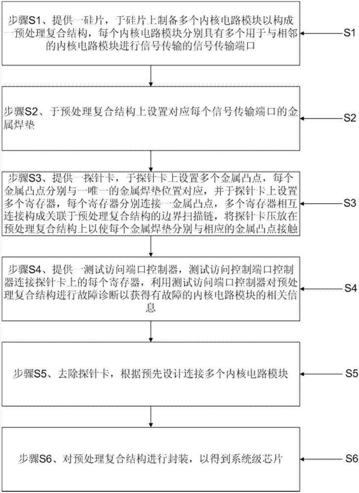
[0043] Such as figure 1 As shown, a system-on-chip production method with fault diagnosis, the above-mentioned method comprises:

[0044] Step S1, providing a silicon chip, preparing a plurality of core circuit modules 1 on the above silicon chip to form a preprocessing composite structure 5, each of the above-mentioned core circuit modules 1 has a plurality of core circuit modules for connecting with adjacent core circuit modules 1. A signal transmission port for signal transmission;

[0045] Step S2, setting metal pads 7 corresponding to each of the above-mentioned signal transmission ports on the above-mentioned pretreatment composite structure 5;

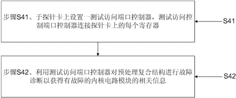
[0046] Step S3, provide a probe card 6, set...


PUM


Abstract

The invention provides a system-on-a-chip (SoC) production method with fault diagnosis. The method comprises the steps of providing a pre-processed composite structure; arranging a metal pad on the pre-processed composite structure; arranging a plurality of metal bumps and a plurality of registers on a probe card, each register being connected with the respective metal bump, the plurality of registers forming a boundary-scan chain, and pressing the probe card on the pre-processed composite structure; completing a fault diagnosis by using a test access port controller to obtain relevant information to a faulty kernel circuit module, then removing the probe card and connecting a plurality of kernel circuit modules; and packaging the pre-processed composite structure. The method of the invention has the beneficial effects of saving the chip area, testing during the manufacturing process, enabling the chip manufacturing to complete the test and discovery in advance, reducing the searchingscope, realizing online positioning of manufacturing defects, reducing the test complexity, and improving the chip testing efficiency, and fault diagnosis coverage and fault diagnosis accuracy.

Description

technical field [0001] The invention relates to the technical field of integrated circuits, in particular to a system-level chip production method with fault diagnosis. Background technique [0002] The basic idea of ​​boundary scan technology is to add a shift register unit on the input and output pins close to the chip. Because these shift register units are distributed on (around) the boundary of the chip, they are called boundary-scan registers (Boundary-Scan Register Cell, BSR). [0003] When the chip is in the debugging state, these boundary scan registers can isolate the input and output of the chip and the periphery. Through these boundary scan register units, the observation and control of the input and output signals of the chip can be realized. For the input pin of the chip, the signal (data) can be loaded into the pin through the connected boundary scan register unit; for the output pin of the chip, it can also be "captured" through the connected boundary scan ...

Claims


Application Information

Patent Timeline
Patent Type & Authority Applications(China)
IPC IPC(8): G01R31/26
CPCG01R31/2601
Inventor 武建宏
Owner SHANGHAI HUALI MICROELECTRONICS CORP
Why Eureka
Try Eureka