OLED film encapsulating structure and encapsulating method

A thin-film encapsulation and loading technology, which is applied in the field of OLED thin-film encapsulation structure and encapsulation, can solve the problems of increased encapsulation film stress, loss of medium contact surface, strong reflection loss, etc., so as to increase light extraction efficiency, prevent thermal damage, and improve usage. effect of life

Active Publication Date: 2018-05-15
WUHAN CHINA STAR OPTOELECTRONICS SEMICON DISPLAY TECH CO LTD
View PDF6 Cites 11 Cited by
  • Summary
  • Abstract
  • Description
  • Claims
  • Application Information

AI Technical Summary

Problems solved by technology

However, as the number of film layers increases, the stress of the packaging film increases, causing the film to crack
At the same time, when light propagates in different media, due to the difference in refractive index, it will reflect on the contact surface of the media and cause loss.
After the light in the OLED passes through the multi-layer film, strong reflection loss will occur. Therefore, there is an urgent need for a thin-film packaging structure that has good water and oxygen barrier properties without affecting the light output efficiency of the OLED.

Method used


Image

  • OLED film encapsulating structure and encapsulating method
  • OLED film encapsulating structure and encapsulating method
  • OLED film encapsulating structure and encapsulating method

Examples


Embodiment Construction

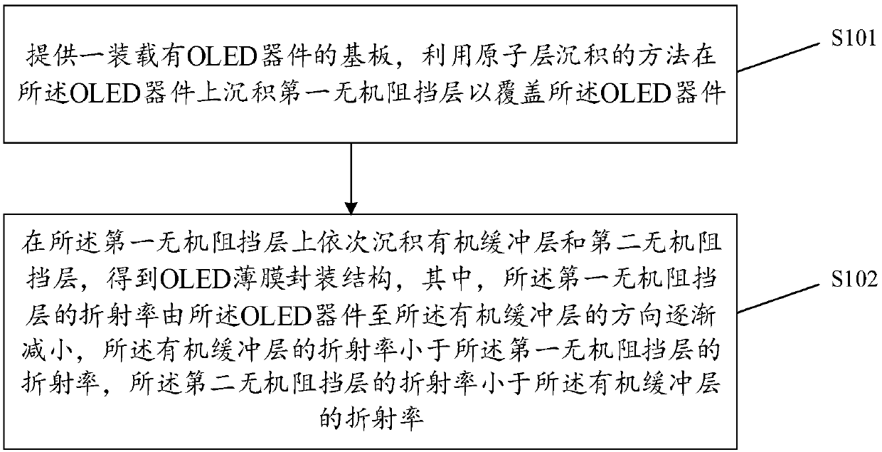
[0023] The following descriptions are preferred implementations of the embodiments of the present invention. It should be pointed out that those skilled in the art can make some improvements and modifications without departing from the principles of the embodiments of the present invention. These improvements And retouching are also regarded as the scope of protection of the embodiments of the present invention.

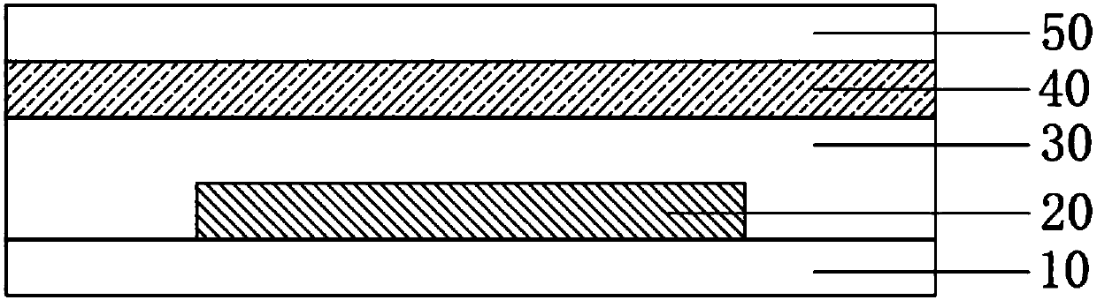
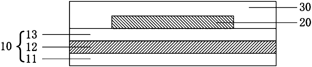
[0024] see figure 1 , an OLED thin film encapsulation structure provided by the present invention, comprising a substrate 10 loaded with an OLED device 20 and a first inorganic barrier layer 30, an organic buffer layer 40 and a second inorganic barrier layer covering the OLED device 20 in sequence 50, the refractive index of the first inorganic barrier layer 30 gradually decreases from the OLED device 20 to the organic buffer layer 40, and the refractive index of the organic buffer layer 40 is smaller than that of the first inorganic barrier layer 30 The refractive ...


PUM


Abstract

The invention provides an OLED film encapsulating structure. The OLED film encapsulating structure comprises a substrate, a first inorganic blocking layer, an organic buffer layer and a second inorganic blocking layer, wherein the substrate is loaded with an OLED device, and the first inorganic blocking layer, the organic buffer layer and the second inorganic blocking layer sequentially cover on the OLED device; and the refraction rate of the first inorganic blocking layer gradually decreases from the OLED device to the organic buffer layer, the refraction rate of the organic buffer layer is lower than that of the first inorganic blocking layer, and the refraction rate of the second inorganic blocking layer is lower than that of the organic buffer layer. By changing the refraction rates ofthe first inorganic blocking layer, the organic buffer layer and the second inorganic blocking layer, the light emitting efficiency of the OLED device can be increased, the situation that external moisture and oxygen penetrate into the OLED device is prevented, the corrosion of internal structures of the OLED device is avoided, meanwhile, a thermal insulation effect is achieved, and thermal damage caused by a subsequent deposition process to the OLED device is prevented; and the organic buffer layer is capable of packaging large-particle foreign matters and simultaneously realizing controlled-release of stress generated during planarization, so that the service life of the device is prolonged.

Description

technical field [0001] The invention relates to the field of display technology, in particular to an OLED film packaging structure and packaging method. Background technique [0002] Organic Light Emitting Diode (OLED) is a new self-luminous display technology, which has the advantages of high brightness and full viewing angle. The metal electrodes in OLED are relatively active, and are easily polluted by water and oxygen in the air, causing black spots on the device, which seriously affects the life of the device. Therefore, the surface of the OLED often needs to be covered with a layer of encapsulation material with excellent water and oxygen blocking effect, so as to improve the service life of the OLED. Therefore, thin film encapsulation technology (TFE) is a necessary encapsulation technology. Film-encapsulated OLED has the advantages of wide color gamut, fast response, high contrast, etc., and has been widely used in the display field. [0003] The currently commonl...

Claims


Application Information

Patent Timeline
Patent Type & Authority Applications(China)
IPC IPC(8): H01L51/52
CPCH10K50/844H10K50/858
Inventor 郭天福
Owner WUHAN CHINA STAR OPTOELECTRONICS SEMICON DISPLAY TECH CO LTD
Why Eureka
Try Eureka