Mixed plasma effect assisted slot waveguide TE mode polarization analyzer

A plasmonic waveguide and plasma technology, applied in the field of integrated optics, can solve problems such as unfavorable production and cost, compression, etc., and achieve the effects of large manufacturing tolerance, high extinction ratio, and low insertion loss

Active Publication Date: 2018-05-18
SOUTHEAST UNIV
View PDF7 Cites 9 Cited by
  • Summary
  • Abstract
  • Description
  • Claims
  • Application Information

AI Technical Summary

Problems solved by technology

However, these structures put forward very high requirements for device manuf

Method used


Image

  • Mixed plasma effect assisted slot waveguide TE mode polarization analyzer
  • Mixed plasma effect assisted slot waveguide TE mode polarization analyzer
  • Mixed plasma effect assisted slot waveguide TE mode polarization analyzer

Examples


Embodiment 1

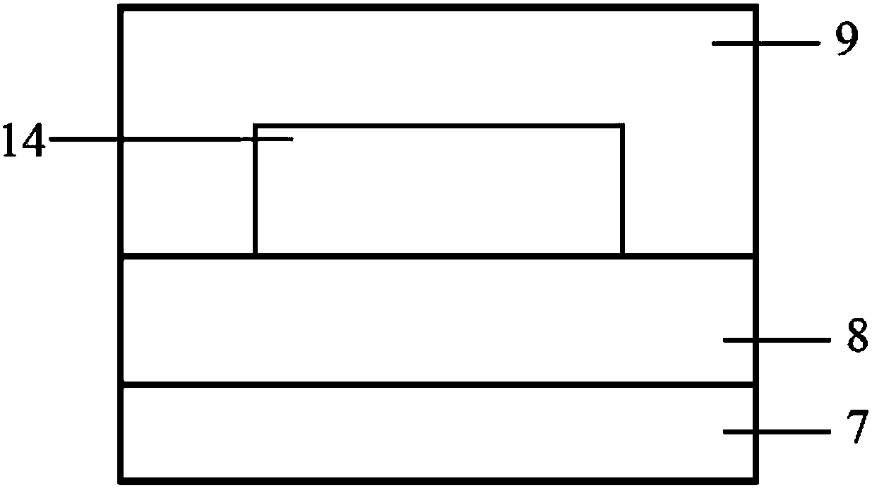
[0038] Such as figure 1 with figure 2 As shown, the analyzer consists of a silicon-based substrate 7, a buried oxide layer 8, an analyzer component 14, and an upper cladding layer 9 from bottom to top, wherein the buried oxide layer 8 is grown on the upper surface of the silicon-based substrate 7, and the upper The cladding layer 9 covers the upper surface of the buried oxide layer 8, and the analyzer component 14 grows horizontally on the upper surface of the buried oxide layer 8 and is covered by the upper cladding layer 9;

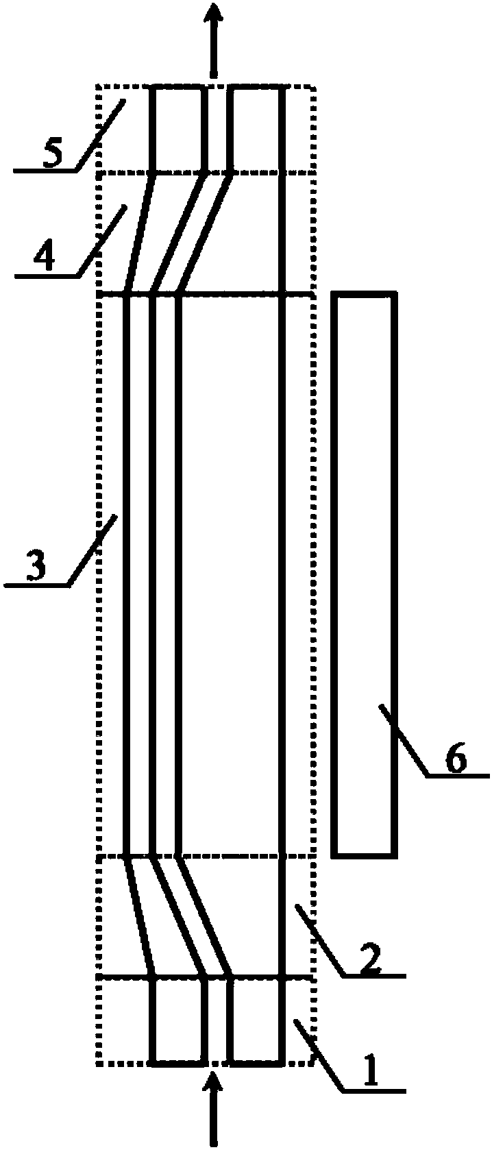
[0039] The polarization analyzer 14 includes an input waveguide 1 for inputting an optical signal, a transition waveguide A2, a through waveguide 3, a transition waveguide B4, an output waveguide 5, and a right through waveguide 6;

[0040] The transition waveguide A2 is connected to one end of the input waveguide 1 and the through waveguide 3; the other end of the through waveguide 3 is connected to the transition waveguide B4; the transition wavegui...


PUM

PropertyMeasurementUnit
Thicknessaaaaaaaaaa

Abstract

The invention discloses a mixed plasma effect assisted slot waveguide TE mode polarization analyzer which successively comprises, from bottom to top, a silicon-base substrate, a buried oxide layer, apolarization analysis component, and an upper cladding layer, wherein the buried oxide layer is grown on the upper surface of the silicon-base substrate, the upper cladding layer covers the upper surface of the buried oxide layer, the polarization analysis component is horizontally grown on the upper surface of the buried oxide layer and covered by the upper cladding layer, and comprises an inputwaveguide, a transition waveguide A, a through waveguide, a transition waveguide B, an output waveguide, and a right through waveguide. The slot waveguide TE polarization analyzer has the advantages of low insertion loss, a high extinction ratio, a large manufacturing tolerance, and a large operating bandwidth.

Description

technical field [0001] The invention relates to a slot-type waveguide TE mode analyzer assisted by a mixed plasma effect, belonging to the technical field of integrated optics. Background technique [0002] The rapid development of optical communication technology and the gradually widening application fields have greatly promoted the research and development of photonic devices. Silicon-based photonic integrated devices have attracted more and more attention from researchers because they are compatible with standard CMOS processes, and have the advantages of low cost, low power consumption, and superior performance. Although the silicon-based material system with high refractive index difference commonly used in integrated photonic devices can effectively reduce the size of the device, it also introduces significant polarization dependence. Therefore, the polarization state of light in the photonic circuit needs to be precisely controlled. As an important waveguide struct...

Claims


Application Information

Patent Timeline
IPC IPC(8): G02B6/126
Inventor 肖金标倪斌
Owner SOUTHEAST UNIV
Why Eureka
Try Eureka