
Photolithography method for silicon wafer surface with high step structure

A silicon wafer surface and step technology, applied in microlithography exposure equipment, optics, optomechanical equipment, etc., can solve the problems of high cost and long operation time, and achieve the effects of short operation time, cost reduction and simple process

Active Publication Date: 2020-03-20
苏州工业园区纳米产业技术研究院有限公司
View PDF5 Cites 0 Cited by
  • Summary
  • Abstract
  • Description
  • Claims
  • Application Information

AI Technical Summary

Problems solved by technology

However, the existing solution requires two exposures and the design of two photomasks to realize the definition of the top of the step and the bottom of the step, which is time-consuming and costly. At the same time, the overlay accuracy and Product impact

Method used


Image

  • Photolithography method for silicon wafer surface with high step structure
  • Photolithography method for silicon wafer surface with high step structure
  • Photolithography method for silicon wafer surface with high step structure

Examples


Embodiment 1

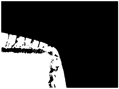
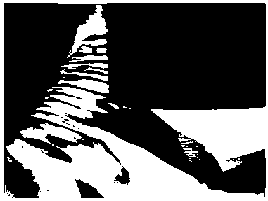
[0038] According to the normal yellow light process, the silicon wafer with a 300μm high step structure wet-etched by KOH is coated with HMDS in an oven, and then a 1:10 ratio of photoresist and solvent is used on the spraying machine. Coat the photoresist on the silicon wafer by spraying, and confirm that the side walls of the steps and the sharp corners are completely covered by the photoresist (see Figure 3 to Figure 6 ), and the glued film at the bottom of the step is confirmed to be 4um, the glued film at the top of the step is confirmed to be 6um, and the thickness of the glued film on the side wall and sharp corner of the step is confirmed to be 2um. Finally, the silicon wafer is placed in a double-sided exposure machine, and the exposure coefficient is adjusted according to the thickness of the adhesive film. At the same time, the exposure treatment is performed on the bottom of the step and the top of the step, and then developed to obtain a photolithographic pattern ...

Embodiment 2

[0040] According to the normal yellow light process, the silicon wafer with a 150 μm high step structure wet etched by KOH is coated with HMDS in an oven, and then a 1:8 ratio of photoresist and solvent is used on the spraying machine. Coat the photoresist on the silicon wafer by spraying, confirm that the side walls and sharp corners of the steps are completely covered by the photoresist, and the coating film at the bottom of the steps is confirmed to be 2um, and the coating film at the top of the steps is confirmed to be 3um , the film thickness of the side wall of the step and the sharp corner is confirmed to be 1um. Finally, the silicon wafer is placed in a double-sided exposure machine, and the exposure coefficient is adjusted according to the thickness of the adhesive film. At the same time, the exposure treatment is performed on the bottom of the step and the top of the step, and then developed to obtain a photolithographic pattern on the bottom of the step and the top o...

Embodiment 3

[0042] According to the normal yellow light process, the silicon wafer with a 500μm high step structure wet-etched by KOH is coated with HMDS in an oven, and then a 1:20 ratio of photoresist and solvent is used on the spraying machine. Coat the photoresist on the silicon wafer by spraying, confirm that the side walls and sharp corners of the steps are completely covered by the photoresist, and the coating film at the bottom of the steps is confirmed to be 6um, and the coating film at the top of the steps is confirmed to be 6um , The film thickness of the side wall of the step and the sharp corner is confirmed to be 4um. Finally, the silicon wafer is placed in a double-sided exposure machine, and the exposure coefficient is adjusted according to the thickness of the adhesive film. At the same time, the exposure treatment is performed on the bottom of the step and the top of the step, and then developed to obtain a photolithographic pattern on the bottom of the step and the top o...


PUM

PropertyMeasurementUnit
heightaaaaaaaaaa
widthaaaaaaaaaa
lengthaaaaaaaaaa

Abstract

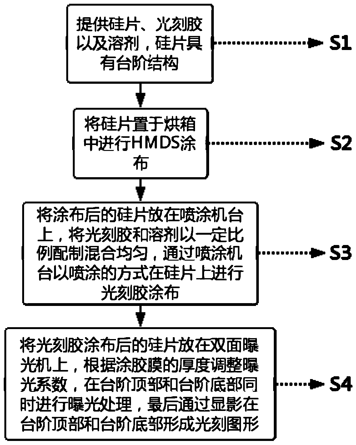
The invention relates to a photoetching method for the surface of a silicon chip of a high step structure and the silicon chip. The photoetching method comprises the following steps: S1, providing thesilicon chip, photoresist and a solvent, wherein the surface of the silicon chip is provided with a step structure; the step structure comprises a step top part, a step bottom part, a step side wallfor connecting the step top part and the step bottom part and a sharp corner; S2, putting the silicon chip into a baking oven for HMDS coating; S3, putting the coated silicon chip onto a spray coatingmachine table; uniformly mixing the photoresist and solvents according to a certain proportion; performing photoresist coating on the silicon chip by the spray coating machine table in a spray coating mode; S4, putting the silicon chip subjected to the photoresist coating onto a double-side exposure machine; regulating the exposure coefficient according to the thickness of a glue coating film; simultaneously performing exposure treatment on the top of the step and the bottom of the step; finally, forming a photoetching pattern on the top of the step and the bottom of the step through development. The photoetching method can achieve the goal of simultaneously realizing the high-resolution ratio patterns at the bottom of the step and the top of the step of the silicon chip of the high-stepstructure.

Description

technical field [0001] The invention relates to a silicon wafer surface photolithography method with a high-step structure, which belongs to the field of micro-electromechanical devices. Background technique [0002] Traditional photolithography is to make photolithographic patterns on the surface of the wafer, that is, planar technology. The existing MEMS applied to the product process of the laser package base will have a high-step structure, which needs to be coated with photoresist on the top and bottom of the structure for protection. However, the existing known methods for obtaining the graphics at the top of the steps and at the bottom of the steps generally adopt the method of multiple exposures. Area occlusion exposes the graphics at the top of the steps, thereby realizing the definition of the graphics at the top of the steps and at the bottom of the steps. However, the existing solution requires two exposures and the design of two photomasks to realize the defin...

Claims


Application Information

Patent Timeline
Patent Type & Authority Patents(China)
IPC IPC(8): G03F7/20H01L21/027
CPCG03F7/70425H01L21/0274
Inventor 蒋丽杨涛
Owner 苏州工业园区纳米产业技术研究院有限公司
Learn More