Semiconductor base, semiconductor device, method for manufacturing semiconductor base, and method for manufacturing semiconductor device
A manufacturing method and semiconductor technology, which are applied in the direction of semiconductor/solid-state device manufacturing, semiconductor devices, electric solid-state devices, etc., to achieve the effect of high pit suppression effect
- Summary
- Abstract
- Description
- Claims
- Application Information
AI Technical Summary
Problems solved by technology
Method used
Image
Examples
Embodiment 1
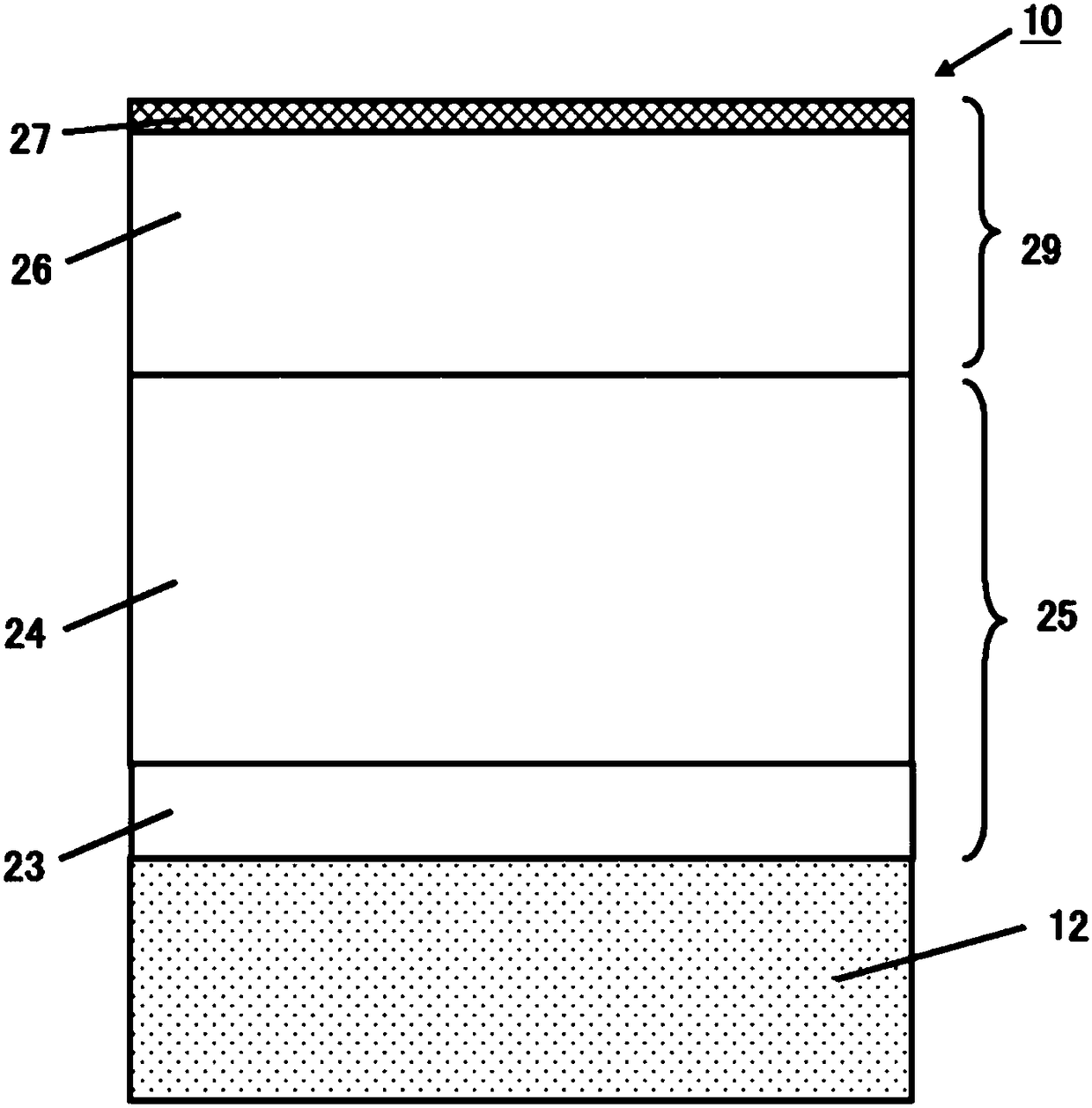
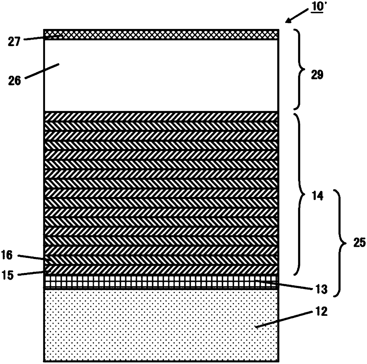
[0093] made as figure 1 Shown semiconductor substrate 10, described semiconductor substrate 10 is provided with buffer layer, and described buffer layer has Image 6 (b) Iron concentration distribution and boron concentration distribution shown. That is, in Example 1, a buffer layer is provided on the substrate 12 made of silicon. The buffer layer is composed of an initial layer made of AlN and a laminate in which GaN layers and AlN layers are alternately laminated. In the buffer layer of Embodiment 1, there is a reduced region and an increased region on the substrate 12, and the reduced region is that the boron concentration changes from the substrate 12 side to the channel layer 26 side by 3×10 19 atoms / cm 3 In a gradually decreasing area, the increasing area is arranged on the decreasing area and the iron concentration is increased from the substrate 12 side to the channel layer 26 side to 5×10 19 atoms / cm 3 In the increased area, after the boron concentration is suffic...
Embodiment 2
[0099] made as figure 1 Shown semiconductor substrate 10, described semiconductor substrate 10 is provided with buffer layer, and described buffer layer has Image 6 (c) The iron concentration distribution and the boron concentration distribution represented. That is, in Example 2, a buffer layer is provided on the substrate 12 made of silicon, and the buffer layer is composed of an initial layer made of AlN and a laminate in which GaN layers and AlN layers are alternately laminated. In the buffer layer of Example 2, there are reduced regions and increased regions on the substrate 12, and the reduced region is that the boron concentration changes from the substrate 12 side to the channel layer 26 side by 3×10 19 atoms / cm 3 In the gradually decreasing area, the increasing area is arranged on the channel layer 26 side from the position where the boron concentration starts to decrease and the iron concentration increases from the substrate 12 side to the channel layer 26 side t...
Embodiment 3
[0105] made as figure 1 Shown semiconductor substrate 10, described semiconductor substrate 10 is provided with buffer layer, and described buffer layer has Image 6 (f) Iron concentration distribution and boron concentration distribution shown. That is, in Example 3, a buffer layer is provided on the substrate 12 made of silicon, and the buffer layer is composed of an initial layer made of AlN and a laminate in which GaN layers and AlN layers are alternately laminated. In the buffer layer of Example 3, there are reduced regions and increased regions on the substrate 12, and the reduced region is that the boron concentration changes from the substrate 12 side to the channel layer 26 side by 3×10 19 atoms / cm 3 In the gradually decreasing area, the increasing area is arranged on the channel layer 26 side from the position where the boron concentration starts to decrease and the iron concentration increases from the substrate 12 side to the channel layer 26 side to 5×10 19 ato...
PUM
 Abstract
Description
Claims
Application Information
 - R&D
- Intellectual Property
- Life Sciences
- Materials
- Tech Scout
- Unparalleled Data Quality
- Higher Quality Content
- 60% Fewer Hallucinations
Browse by: Latest US Patents, China's latest patents, Technical Efficacy Thesaurus, Application Domain, Technology Topic, Popular Technical Reports.
© 2025 PatSnap. All rights reserved.Legal|Privacy policy|Modern Slavery Act Transparency Statement|Sitemap|About US| Contact US: help@patsnap.com


