Storage module on basis of VPX single-slot structure
A memory module and single-slot technology, applied in static memory, data processing input/output process, instruments, etc., can solve the problems of product integration, failure to meet performance requirements, large volume, etc., to achieve capacity and bandwidth expansion , rich interface, the effect of reducing the volume
- Summary
- Abstract
- Description
- Claims
- Application Information
AI Technical Summary
Problems solved by technology
Method used
Image
Examples
Embodiment 1
[0050] In the high-speed data acquisition and playback system, in order to meet the data storage rate and capacity requirements, the storage module is required to have extremely high data read and write bandwidth. The size of the storage module matched in the standard chassis is required to be controlled, and the bandwidth and capacity required by the system must be realized in one slot. It is very difficult to improve the structural design, heat dissipation design, circuit design, and software design of the storage module in the prior art.
[0051] The invention can be applied in occasions requiring high-speed data collection and playback, such as radar and communication. The invention realizes 16TB storage capacity and 6Gb / s data reading and writing bandwidth in a standard 6U 5HP slot based on the 6Gb / s storage module of the VPX single-slot structure.
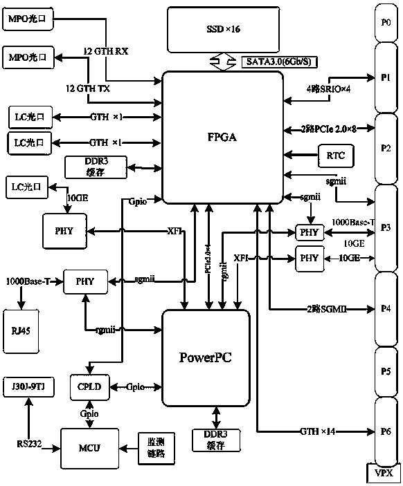
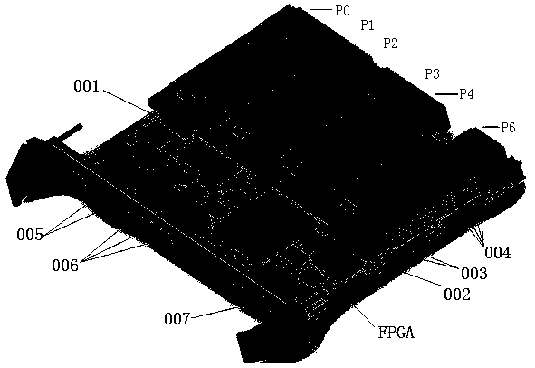
[0052] Such as figure 1 , figure 2 , image 3 As shown, a storage module based on a VPX single-slot structure is based...
Embodiment 2
[0068] This embodiment is optimized on the basis of Embodiment 1 or Embodiment 2, and the storage module further includes an MCU.
[0069] The model of the MCU is STM32F405RCT6, and the typical power consumption is 0.5W. Using the characteristics of STM32F405 processor, such as multiple IIC interfaces and low power consumption, a state monitoring and management signal channel in the board based on IIC bus is established. This bus mainly monitors the working status of main functional chips such as FPGA, PowerPC, interface chip, and optical module in the board, forms a general data frame, and broadcasts to the outside through the IIC interface on VPX P0.
[0070] Such as figure 1 As shown, the MCU is connected to the J30J-9TJ interface through RS232. J30J-9TJ is a debugging interface, including a serial port, which can be used to monitor and record the internal working status of the playback module and other information.
[0071] Such as figure 1 As shown, the RJ45 is connec...
Embodiment 3
[0073] This embodiment is optimized on the basis of Embodiment 1 or Embodiment 2. The standard connector of the VPX is provided with six interface connectors, P0, P1, P2, P3, P4, and P6. P0~P6 are standard connectors for VPX structural boards, used to connect VPX boards to the chassis backplane. Various high-speed signal interfaces are defined on these connectors, such as SRIO, PCIE, 10GbE, Aurora, etc.
[0074] P0 is a standard power supply connector, and P5 is not used. The FPGA is connected to the P1 interface through 4-way RapidIO×4, the FPGA is connected to the P2 interface through 2-way PCIe 2.0×8, and the FPGA is connected to the P3 interface through 2-way Gigabit network and 1-way 10-Gigabit network. The FPGA is connected to the P4 interface through 2-way SGMII, and the FPGA is connected to the P6 interface through 14-way GTH. The 10G interface and 1000Base-T interface on the P3 interface connector are designed to provide a rich control and management interface to th...
PUM
 Abstract
Description
Claims
Application Information


