
Broadband electrically tunable absorber based on graphene double rings

A double-ring and graphene technology, applied in the direction of instruments, electrical components, antennas, etc., can solve the problems of narrow absorbing range, limit the practical application of metamaterial absorbing structures, constant performance and response, and achieve expansion Wide bandwidth, good broadband absorption effect, effect of ensuring polarization independence

Inactive Publication Date: 2018-06-19
SHANGHAI INST OF OPTICS & FINE MECHANICS CHINESE ACAD OF SCI
View PDF6 Cites 16 Cited by
  • Summary
  • Abstract
  • Description
  • Claims
  • Application Information

AI Technical Summary

Problems solved by technology

This resonance-based metamaterial absorber structure has the advantages of small size, and the resonance band can be adjusted through the structural size. However, due to the intrinsic defects of the resonance response, the absorbing range that can be achieved is very narrow. In many practical applications not applicable
In addition, most of the metamaterial absorbing structures use metal as the resonant structural unit, which means that once the structure is processed, its performance and response are fixed. These defects greatly limit the practical application of metamaterial absorbing structures.

Method used


Image

  • Broadband electrically tunable absorber based on graphene double rings
  • Broadband electrically tunable absorber based on graphene double rings
  • Broadband electrically tunable absorber based on graphene double rings

Examples


Embodiment Construction

[0034] The present invention will be further described in detail below in conjunction with the accompanying drawings and examples, but the protection scope of the present invention should not be limited thereto.

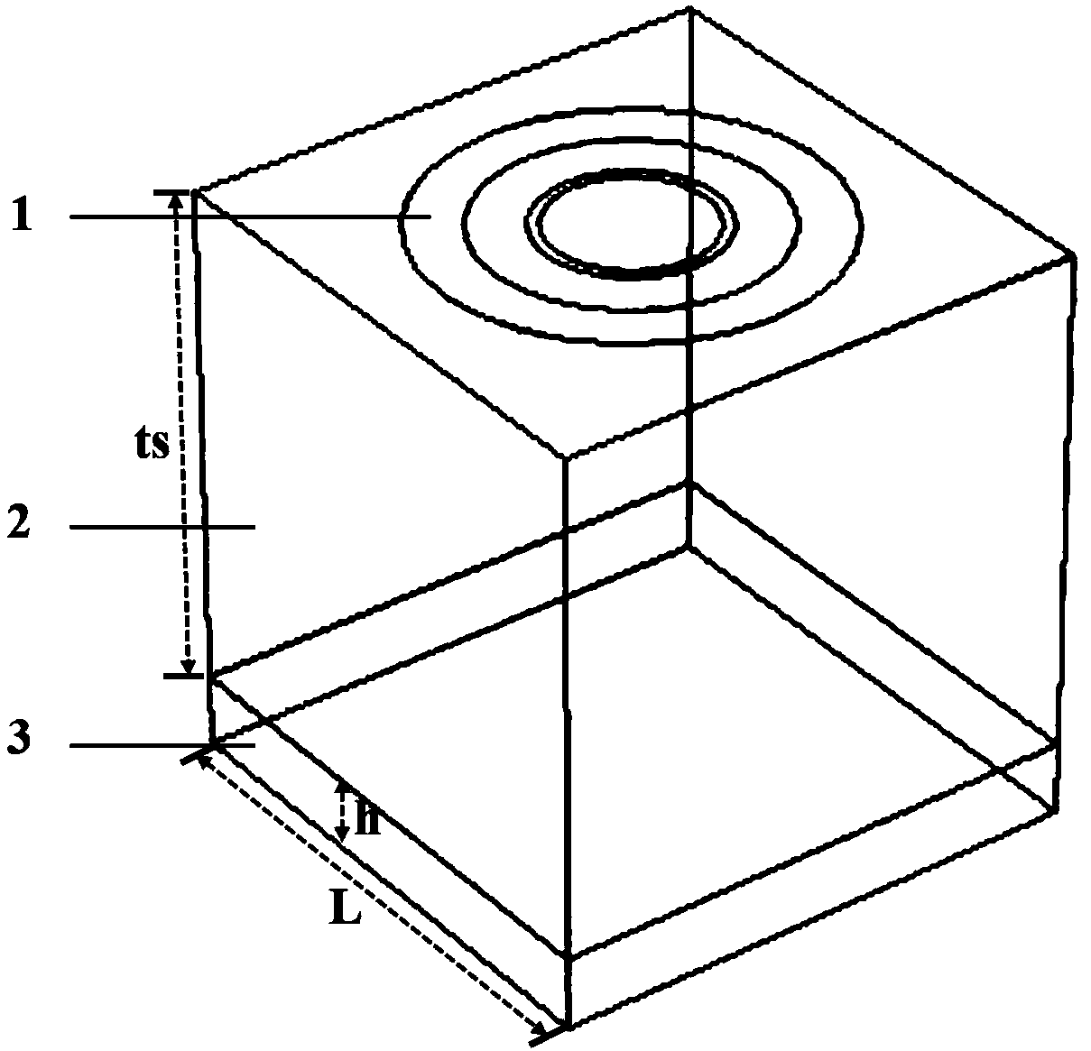
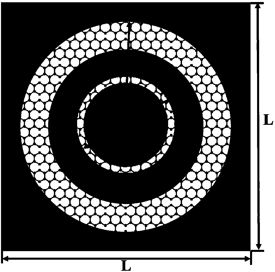
[0035] see figure 1 , figure 1 It is a schematic diagram of the unit structure of the absorber. As shown in the figure, a broadband absorber based on a graphene double-ring structure uses a metal 3 as a reflective substrate, and the structure is followed by an insulating dielectric layer 2 and a graphene layer 1. , the graphene layer is composed of periodic single-layer graphene double ring structure. Gold with high conductivity is used as the structural substrate to realize a completely reflective structure. The thickness of gold is greater than 100nm (greater than the skin depth), and the reflection loss of the gold film in the terahertz band is very small. In the simulation, it can be regarded as a perfect electric conductor (PEC). figure 2 A top view of the to...


PUM


Abstract

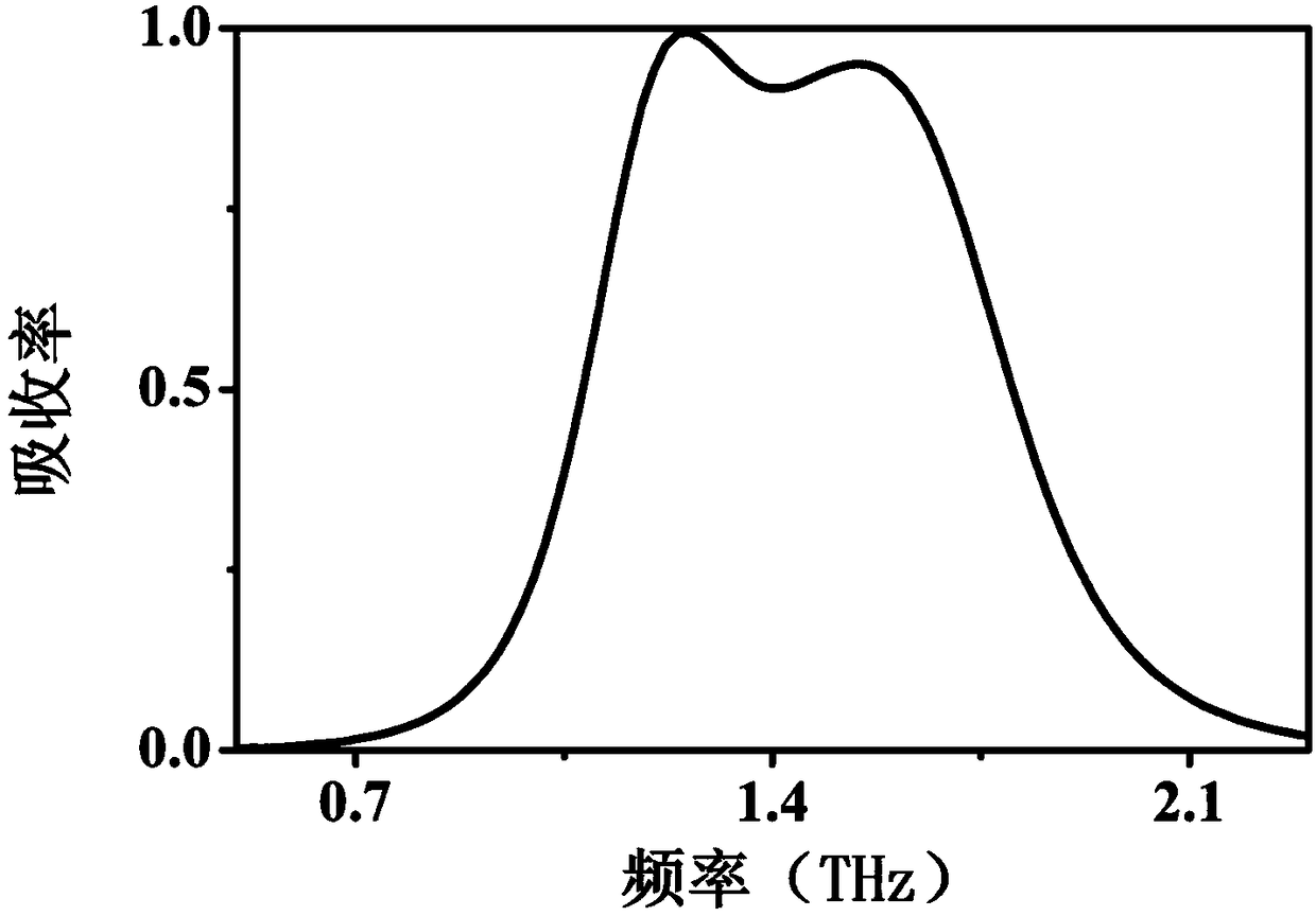
The invention discloses a broadband absorber based on a double-ring structure of graphene. With metal as a reflective substrate, an insulating dielectric layer and a graphene layer are above the reflective substrate in order. The graphene layer is formed by a periodic monolayer graphene double-ring structure. Since the graphene exhibits strong metallicity in infrared and terahertz bands, a graphene structure is directly used as a resonant structural unit, a strong resonance coupling between graphene nanostructures realizes a single-layer broadband absorber, and the processing process of the structure is greatly simplified. Because of the unique electrical properties of the graphene, a chemical potential and a surface conductivity can be changed by the change of applied bias voltage, and the absorption frequency range of an absorbing structure is regulated. The broadband absorber has the advantages of a simple structure and high absorption efficiency and has important application prospects in the fields of terahertz imaging, sensing, a continuous light source and the like.

Description

technical field [0001] The invention relates to the field of electromagnetic wave absorption, in particular to a broadband electrically adjustable wave absorber based on a single-layer graphene structure. The structure of the absorber can realize the characteristics of broadband absorbing, wide-band adjustable absorbing range, large-angle broadband absorbing and polarization unknown, and can be used for sensor design in the terahertz band, terahertz imaging, terahertz light source, etc. Background technique [0002] Electromagnetic absorbing material is a kind of material that reduces the reflection and transmittance of electromagnetic waves incident on it, absorbs electromagnetic waves through internal loss, and converts electromagnetic wave energy into other forms of energy. Because of its very important applications in many fields such as solar cells, photoelectric detection, electromagnetic stealth, and electromagnetic radiation, it has attracted extensive attention from...

Claims


Application Information

Patent Timeline
IPC IPC(8): H01Q17/00G02B5/00
CPCG02B5/003H01Q17/007H01Q17/008
Inventor 张龙牟南历董红星姜雄伟张亚强
Owner SHANGHAI INST OF OPTICS & FINE MECHANICS CHINESE ACAD OF SCI
Learn More