
A kind of zener diode and its manufacturing method

A Zener diode and electrode technology, applied in the field of Zener diodes and their manufacturing, can solve the problems of the breakdown voltage of the Zener diode, the influence of resistance, the small resistance of the Zener diode, etc., so as to improve the stability and reduce the dynamic resistance. Effect

Active Publication Date: 2021-07-13
NANJING SILERGY SEMICON TECH CO LTD
View PDF4 Cites 0 Cited by
  • Summary
  • Abstract
  • Description
  • Claims
  • Application Information

AI Technical Summary

Problems solved by technology

[0005] Therefore, the breakdown voltage and resistance of prior art zener diodes are affected by the thickness of the lightly doped epitaxial layer
On the premise of keeping the resistance of the Zener diode small, it is challenging to obtain a high and stable breakdown voltage

Method used


Image

  • A kind of zener diode and its manufacturing method
  • A kind of zener diode and its manufacturing method
  • A kind of zener diode and its manufacturing method

Examples


Embodiment Construction

[0035] Hereinafter, the present invention will be described in more detail with reference to the accompanying drawings. In the various figures, identical elements are indicated with similar reference numerals. For the sake of clarity, various parts in the drawings have not been drawn to scale. Also, some well-known parts may not be shown. For the sake of simplicity, the semiconductor structure obtained after several steps can be described in one figure.

[0036] It should be understood that when describing the structure of a component, when a layer or a region is referred to as being "on" or "over" another layer or another region, it may mean being directly on another layer or another region, or Other layers or regions are also included between it and another layer or another region. And, if the part is turned over, the layer, one region, will be "below" or "beneath" the other layer, another region.

[0037] If it is to describe the situation directly on another layer or a...


PUM

PropertyMeasurementUnit
thicknessaaaaaaaaaa
electrical resistivityaaaaaaaaaa

Abstract

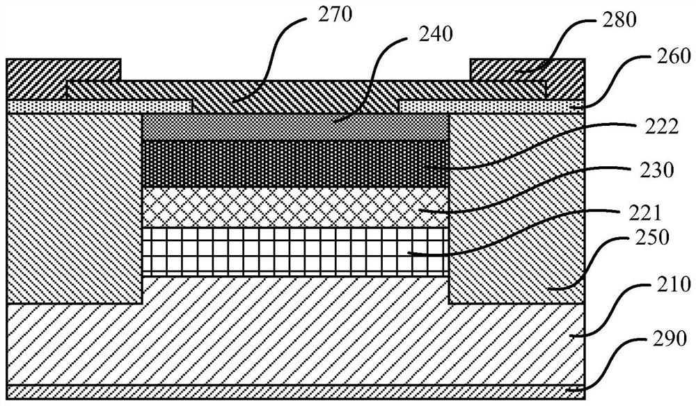
The present application discloses a Zener diode and its manufacturing method, comprising: a semiconductor substrate; a first epitaxial layer located on the semiconductor substrate; a well region located in the first epitaxial layer; a second epitaxial layer located on the well region The doping region is located in the second epitaxial layer, wherein the semiconductor substrate, the first epitaxial layer, and the well region are respectively of the first doping type, the doping region is of the second doping type, and the first doping type and the second doping type The two doping types are opposite, and the doping concentration of the first epitaxial layer is higher than that of the second epitaxial layer. The first doping type is one of N-type and P-type, and the second doping type is the other of N-type and P-type. The zener diode can simultaneously improve the stability of the breakdown voltage and reduce the dynamic resistance by adding the second epitaxial layer and forming a well region by high-energy ion implantation in the first epitaxial layer.

Description

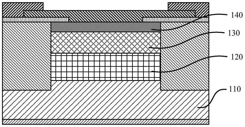
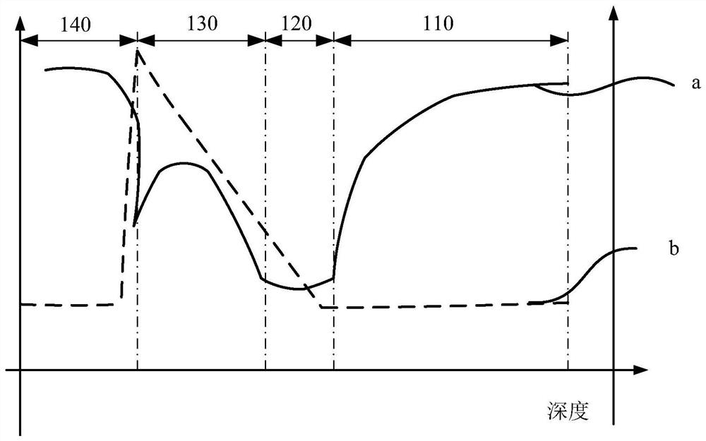
technical field [0001] The invention relates to the technical field of semiconductor manufacturing, and more particularly relates to a Zener diode and a manufacturing method thereof. Background technique [0002] The structure diagram of Zener diode in the prior art is as follows Figure 1a As shown, it includes a heavily doped semiconductor substrate 110, a lightly doped epitaxial layer 120, a well region 130, and a doped region 140. The doping type of the region 130 is opposite, forming a PN junction between the well region 130 and the doped region 140 . In order to obtain a higher breakdown voltage, the thermal diffusion time needs to be increased to ensure that the depth of the well region 130 is greater than the width of the depletion layer in the epitaxial layer 120 when the junction breaks down. When the well region 130 diffuses in the epitaxial layer, the doping impurities of the heavily doped semiconductor substrate 110 will also diffuse from the bottom of the epit...

Claims


Application Information

Patent Timeline
Patent Type & Authority Patents(China)
IPC IPC(8): H01L29/06H01L29/866H01L21/329
CPCH01L29/0619H01L29/0684H01L29/6609H01L29/866
Inventor 殷登平赵豹王世军姚飞
Owner NANJING SILERGY SEMICON TECH CO LTD
Learn More