Exit pupil-expanding compact type nano-structure waveguide display method and system

A technology of nanostructure and display method, which can be applied to optical waveguides, optics, instruments, etc., can solve the problems of inability to expand the exit pupil effect, limitation of light exit pupil diameter, complex system structure, etc., so as to improve the diffraction efficiency and the field of view. , The output beam is uniform and the effect of reducing the volume of the system

Active Publication Date: 2018-06-29
BEIJING INSTITUTE OF TECHNOLOGYGY
View PDF11 Cites 4 Cited by
  • Summary
  • Abstract
  • Description
  • Claims
  • Application Information

AI Technical Summary

Problems solved by technology

[0005] The present invention provides a waveguide display method and system in order to solve the problem that the existing waveguide display system has a complicated system structure, and at the same time, the diameter of the light exit pupil is limited, and the effect of expanding the exit pupil cannot be realized with a simple waveguide display structure.

Method used


Image

  • Exit pupil-expanding compact type nano-structure waveguide display method and system
  • Exit pupil-expanding compact type nano-structure waveguide display method and system
  • Exit pupil-expanding compact type nano-structure waveguide display method and system

Examples


Embodiment Construction

[0026] The specific implementation manners of the present invention will be further described in detail below in conjunction with the accompanying drawings and embodiments. The following examples are used to illustrate the present invention, but are not intended to limit the scope of the present invention.

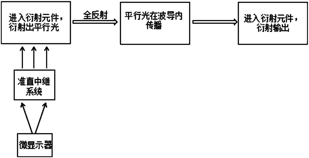
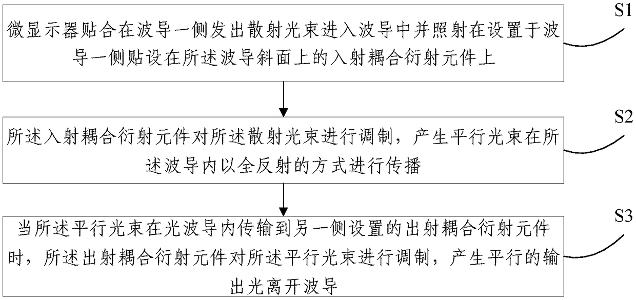
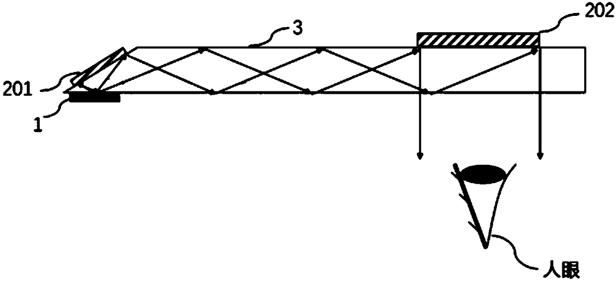
[0027] refer to figure 2 , figure 2 It is a flow chart of a method for displaying a compact nanostructure waveguide with enlarged exit pupil provided by an embodiment of the present invention. The method includes:

[0028] S1, attaching the micro-display on one side of the waveguide to emit a scattered beam into the waveguide and irradiating it on the in-coupling diffraction element arranged on the side of the waveguide and attached to the slope of the waveguide;

[0029] S2 The in-coupling diffraction element modulates the scattered light beam to generate parallel light beams that propagate in the waveguide in a manner of total reflection;

[0030] S3 When the parall...


PUM


Abstract

The invention provides an exit pupil-expanding compact type nano-structure waveguide display method and an exit pupil-expanding compact type nano-structure waveguide display system. The method comprises the following steps: a microdisplay clings to one side of the waveguide to emit scattered beams, and the scattered beams enter the waveguide and are irradiated on an incident coupling diffraction component arranged on one side of the waveguide and clings to the inclined surface of the waveguide; the incident coupling diffraction component modulates the scattered beams to generate parallel beamsto be propagated in the waveguide in a total reflection mode; and when the parallel beams in the light waveguide are transmitted to an emergent coupling diffraction component arranged on the other side, the emergent coupling diffraction component modulates the parallel beams to generate parallel output light to depart from the waveguide. According to the method provided by the invention, a collimating device between the microdisplay and the waveguide is removed, so the structure required by waveguide display is simplified; meanwhile, one incline surface is arranged at one end of the waveguideand the incident coupling diffraction component is arranged on the inclined surface, so that the diffraction efficiency and the field angle of the display system are improved and the exit pupil diameter is enlarged.

Description

technical field [0001] The invention relates to the field of optical waveguide display, in particular to a method and system for expanding the exit pupil and compact nanostructure waveguide display. Background technique [0002] The diffractive waveguide display method combines micro-nano, holographic and other diffraction technologies with waveguide technology. Through the diffraction effect of the diffraction element, the amplitude or phase of the light wave is modulated, and the waveguide is used to propagate the light wave in a directional way, so that the virtual image can be projected and The purpose of overlaying external scene images together. This method effectively solves the problem of off-axis transmission of the optical path, and has the advantages of small volume, light weight and the like. In the diffractive waveguide display technology, the diffractive element acts as an optical lens. Compared with ordinary glass lenses, diffractive optical elements provide...

Claims


Application Information

Patent Timeline
Patent Type & Authority Applications(China)
IPC IPC(8): G02B6/10G02B27/42
Inventor 刘娟施学良
Owner BEIJING INSTITUTE OF TECHNOLOGYGY
Why Eureka
Try Eureka