Chip packaging structure and method
A chip packaging structure, chip technology, applied in the direction of semiconductor/solid-state device components, semiconductor devices, electrical components, etc., can solve the problems of unstable adhesive thickness, unstable process, low efficiency, etc., to improve mechanical strength and Reliability, shortening process time, effect of reducing process steps
- Summary
- Abstract
- Description
- Claims
- Application Information
AI Technical Summary
Problems solved by technology
Method used
Image

Examples
Embodiment 1
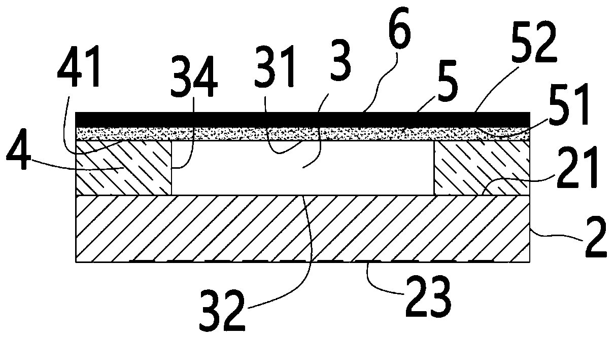
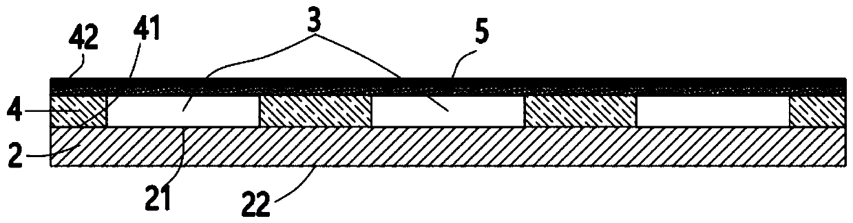
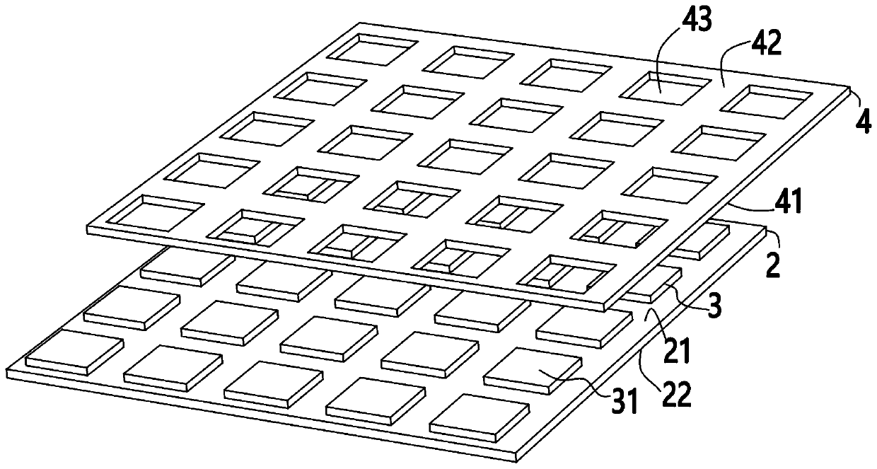
[0078] Please refer to figure 1 What is shown is a schematic cross-sectional view of the state after the chip packaging structure is packaged. The bottom of the chip is the substrate 2 for mounting the chip. The chip is electrically connected to the substrate 2 and fixed. The corelayer (metal layer) under the soldermask (solder mask), and the soldermask (solder mask) under the metal layer, the soldermask (solder mask) is used to protect the corelayer (metal layer) in the middle, preventing the corelayer (metal layer) ) problems such as short circuits occur in the welding process, and the thickness of the multi-layer substrate is between 100 microns and 300 microns. The chip includes a functional surface 31 and a non-functional surface 32 opposite to the functional surface. The functional surface 31 contains circuits for performing target functions, including sensing components and driving circuits for sensing fingerprint characteristics. The functional surface 31 is arranged ...
Embodiment 2
[0128] refer to Figure 5a and Figure 5b Compared with Embodiment 1, the difference in technical solution is that in step S4
[0129] Before the hard cover, the filling material and the substrate on which the chip is fixed are put into the film lamination equipment, the filling material and the hard cover 6 are bonded in advance. Follow the steps:
[0130] S41: paste the release film 15 in the first mold 11 of the compression molding equipment
[0131] S42: Put the hard cover plate 6 on the release film 15 in the first mold, with the first surface 61 facing upward;
[0132] S43: placing the packaging compound 51 on the first surface 61 of the hard cover 6;
[0133] S44: fixing the substrate 2 on which the chip 3 is fixed on the second mold 12;
[0134] S45: Clamp the second mold 12 and the first mold 11, vacuumize and heat, so that the encapsulation material 51 is cured to form the encapsulation layer 5;
[0135] S46: demoulding to obtain the package structure of the ch...
Embodiment 3
[0138] refer to Figure 6a and Figure 6b The difference from Embodiment 1 or Embodiment 2 is that in step S4, the encapsulating material 51 is not pre-placed in the molding device 1 but is a fluid encapsulating material injected after vacuuming and heating, specifically including steps:
[0139] S41: paste the release film 15 in the first mold of the compression molding equipment;
[0140] S42: Put the hard cover plate 6 on the release film in the first mold 11, with the first surface 61 facing upward;
[0141] S43: fixing the substrate 2 on which the chip 4 is fixed on the second mold 12;
[0142] S44: Clamp the second mold 12 and the first mold 11, vacuumize and heat, inject the fluid encapsulation compound 51, and solidify the encapsulation compound to form the encapsulation layer 5;
[0143] S45: demoulding to obtain a chip packaging structure.
[0144] The rest of the structures and packaging methods are the same as those in Embodiment 1, and will not be repeated her...
PUM
| Property | Measurement | Unit |
|---|---|---|
| thickness | aaaaa | aaaaa |
| thickness | aaaaa | aaaaa |
Abstract
Description
Claims
Application Information
 - R&D
- Intellectual Property
- Life Sciences
- Materials
- Tech Scout
- Unparalleled Data Quality
- Higher Quality Content
- 60% Fewer Hallucinations
Browse by: Latest US Patents, China's latest patents, Technical Efficacy Thesaurus, Application Domain, Technology Topic, Popular Technical Reports.
© 2025 PatSnap. All rights reserved.Legal|Privacy policy|Modern Slavery Act Transparency Statement|Sitemap|About US| Contact US: help@patsnap.com