Semiconductor device, manufacturing method thereof and electronic device
A manufacturing method and semiconductor technology, applied in the direction of semiconductor devices, semiconductor/solid-state device components, electric solid-state devices, etc., can solve the problems of small area, small number of turns, and multi-chip area of inductive devices, so as to improve the inductance coefficient, inductance Capability enhancement, the effect of improving RF performance
- Summary
- Abstract
- Description
- Claims
- Application Information
AI Technical Summary
Problems solved by technology
Method used
Image

Examples
Embodiment 1
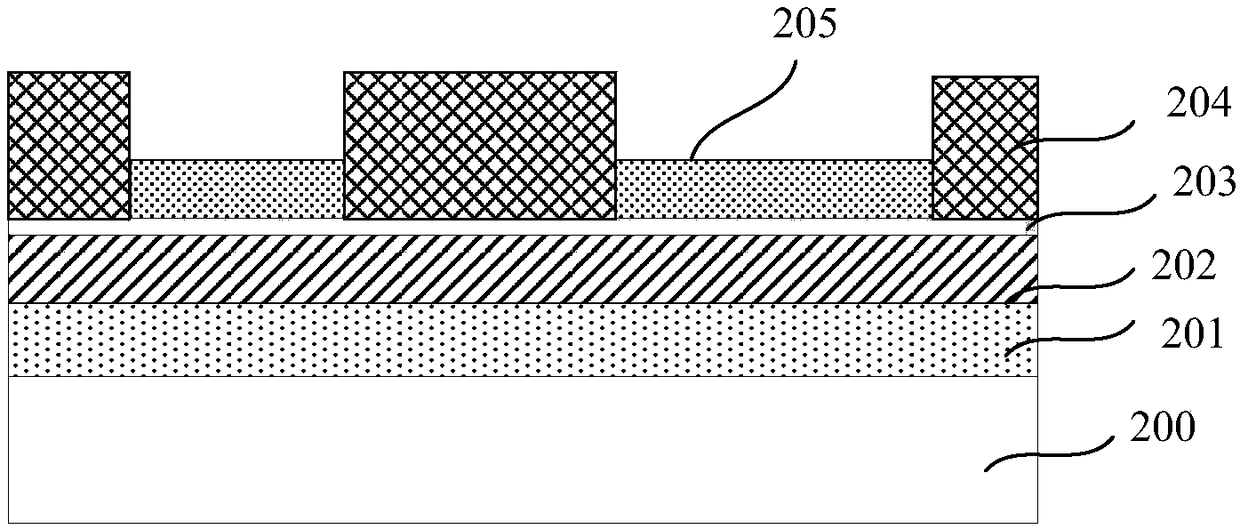
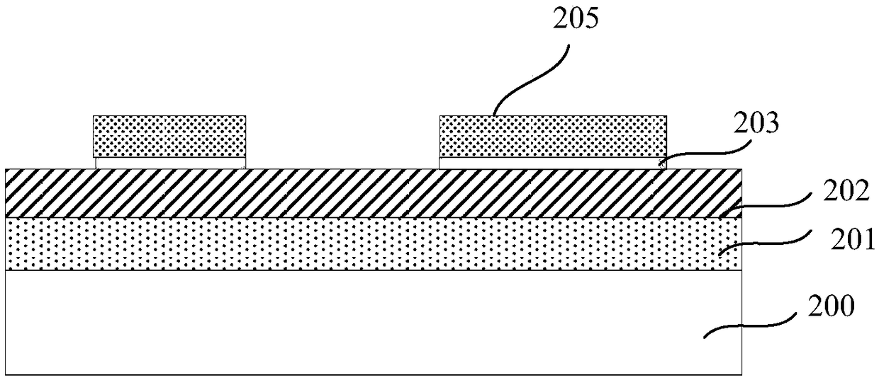
[0040] The following will refer to figure 1 , Figure 2A ~ Figure 2G as well as image 3 A method for fabricating a semiconductor device according to an embodiment of the present invention will be described in detail.
[0041] First, step 101 is performed to provide a device wafer, the device wafer includes a semiconductor substrate 200 and a device layer 201, an isolation layer 202 is formed on the device wafer, and a first barrier layer is formed on the isolation layer And / or seed layer 203, on described first barrier layer and / or seed layer 203, form the patterned photoresist layer 204 of Li, and carry out copper electroplating with the photoresist layer 204 of described pattern as mask process to form the first metal layer 205, the formed structure is as Figure 2A shown.
[0042] The semiconductor substrate 200 can be at least one of the materials mentioned below: Si, Ge, SiGe, SiC, SiGeC, InAs, GaAs, InP or other III / V compound semiconductors, and also includes multi...
Embodiment 2
[0072] The present invention also provides a semiconductor device, such as Figure 4As shown, the semiconductor device includes: a device wafer, the device wafer includes a semiconductor substrate 400 and a device layer 401, an isolation layer 402 is formed on the device wafer, and multiple layers are formed on the isolation layer 402 Layer stacked structure, each layer of stacked structure includes a layer of metal layer 403 and a layer of dielectric layer 404 covering the metal layer, multiple layers of the metal layer 403 form at least one inductor coil structure, in the dielectric layer 404 and each A magnetic core 405 is formed at a position corresponding to the central area of the inductor coil structure.
[0073] Wherein, the semiconductor substrate 400 can be at least one of the materials mentioned below: Si, Ge, SiGe, SiC, SiGeC, InAs, GaAs, InP or other III / V compound semiconductors, and also includes multiple semiconductors composed of these semiconductors. The l...
Embodiment 3
[0079] Still another embodiment of the present invention provides an electronic device, including a semiconductor device and an electronic component connected to the semiconductor device. Wherein, the semiconductor device includes: a device wafer, an isolation layer is formed on the device wafer, a multi-layer stack structure is formed on the isolation layer, each layer stack structure includes a metal layer and a layer covering the A dielectric layer of the metal layer, wherein multiple layers of the metal layer form at least one inductive coil structure, and a magnetic core is formed in the dielectric layer at a position corresponding to a central area of each inductive coil structure.
[0080] Wherein, the device wafer includes a semiconductor substrate and a device layer. The semiconductor substrate can be at least one of the materials mentioned below: Si, Ge, SiGe, SiC, SiGeC, InAs, GaAs, InP or other III / V compound semiconductors, including multilayer structures compos...
PUM
 Abstract
Description
Claims
Application Information
 - R&D
- Intellectual Property
- Life Sciences
- Materials
- Tech Scout
- Unparalleled Data Quality
- Higher Quality Content
- 60% Fewer Hallucinations
Browse by: Latest US Patents, China's latest patents, Technical Efficacy Thesaurus, Application Domain, Technology Topic, Popular Technical Reports.
© 2025 PatSnap. All rights reserved.Legal|Privacy policy|Modern Slavery Act Transparency Statement|Sitemap|About US| Contact US: help@patsnap.com