
Alloy material possessing quantum well energy level structure, manufacturing method and semiconductor device

An alloy material and energy level structure technology, applied in the field of quantum dots, can solve the problems of inability to meet the requirements of semiconductor devices and the luminous performance needs to be improved, and achieve the effect of meeting the comprehensive performance requirements and high luminous efficiency

Active Publication Date: 2018-07-10
TCL CORPORATION
View PDF14 Cites 1 Cited by
  • Summary
  • Abstract
  • Description
  • Claims
  • Application Information

AI Technical Summary

Problems solved by technology

[0013] In view of the above-mentioned deficiencies in the prior art, the object of the present invention is to provide an alloy material with a quantum well level structure, a preparation method and a semiconductor device, aiming at solving the problem that the existing quantum dot material needs to be improved in its luminous performance and cannot meet the requirements of semiconductor devices. Questions about the requirements of quantum dot materials

Method used


Image

  • Alloy material possessing quantum well energy level structure, manufacturing method and semiconductor device
  • Alloy material possessing quantum well energy level structure, manufacturing method and semiconductor device
  • Alloy material possessing quantum well energy level structure, manufacturing method and semiconductor device

Examples


preparation example Construction

[0069] The present invention also provides a method for preparing the above-mentioned alloy material, which comprises the steps of:

[0070] Synthesizing a first compound at a predetermined location;

[0071] synthesizing a second compound on the surface of the first compound, the alloy composition of the first compound and the second compound being the same or different;

[0072] A cation exchange reaction occurs between the first compound and the second compound to form an alloy material, and the luminescence peak wavelength of the alloy material has intermittent blue shift.

[0073] The preparation method of the present invention combines the quantum dot SILAR synthesis method with the quantum dot one-step synthesis method to generate alloy materials, specifically, the quantum dots are grown layer by layer and the quantum dot one-step synthesis method is used to form a transition shell with a gradual composition. That is to say, two compound thin layers with the same or di...

Embodiment 1

[0100] Embodiment 1: Preparation based on CdZnSeS / CdZnSeS quantum dots

[0101] The precursors of cation Cd, cation Zn, anion Se and anion S are injected into the reaction system to form Cd y Zn 1-y Se b S 1-b Layer (where 0≤y≤1, 0≤b≤1); continue to inject the precursors of cation Cd, cation Zn, anion Se and anion S into the reaction system, in the above Cd y Zn 1-y Se b S 1-b Cd z Zn 1-z Se c S 1-c layer (where 0≤z≤1, and z is not equal to y, 0≤c≤1); under certain reaction conditions such as heating temperature and heating time, Cd and The exchange of Zn ions; because the migration distance of cations is limited and the probability of migration is smaller the farther the migration distance is, so it will be in Cd y Zn 1-y Se b S 1-b layer with Cd z Zn 1-z Se c S 1-c A graded alloy composition distribution of Cd content and Zn content is formed near the interface of the layer, that is, Cd x Zn 1-x Se a S 1-a , where 0≤x≤1, 0≤a≤1.

Embodiment 2

[0102] Embodiment 2: Preparation based on CdZnS / CdZnS quantum dots

[0103] The precursors of cation Cd, cation Zn and anion S are injected into the reaction system to form Cd y Zn 1-y S layer (where 0≤y≤1); continue to inject the precursor of cation Cd, the precursor of cation Zn and the precursor of anion S into the reaction system, the above Cd y Zn 1-y Cd formed on the surface of the S layer z Zn 1-z S layer (where 0≤z≤1, and z is not equal to y); under certain reaction conditions such as heating temperature and heating time, the exchange of Cd and Zn ions in the inner and outer nanocrystals (that is, the above two-layer compound) occurs ; Since the migration distance of cations is limited and the farther the migration distance is, the probability of migration is smaller, so the Cd y Zn 1-y S layer and Cd z Zn 1-z A gradual alloy composition distribution of Cd content and Zn content is formed near the interface of the S layer, that is, Cd x Zn 1-x S, where 0≤x≤1....


PUM


Abstract

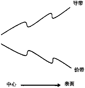
The invention discloses an alloy material possessing a quantum well energy level structure, a manufacturing method and a QLED. The alloy material contains N structure units which are successively arranged along a radial direction, wherein the N is greater than or equal to 1. Each structural unit is a graded alloy component structure in which an energy level width becomes wider from inside to outside in the radial direction. The energy level widths of the adjacent structure units are not continuous. The invention provides the novel alloy material having a mutated alloy component along the radial direction from the inside to the outside. High-efficient luminescence efficiency is realized, simultaneously the comprehensive property requirements of a QLED device and a corresponding display technology to the alloy material can be satisfied. The material is an ideal alloy material suitable for the QLED device and the display technology.

Description

technical field [0001] The invention relates to the field of quantum dots, in particular to an alloy material with a quantum well energy level structure, a preparation method and a semiconductor device. Background technique [0002] Quantum dots are a special material that is confined to the order of nanometers in three dimensions. This remarkable quantum confinement effect makes quantum dots have many unique nanometer properties: continuously adjustable emission wavelength, narrow emission wavelength, Broad absorption spectrum, high luminous intensity, long fluorescence lifetime and good biocompatibility, etc. These characteristics make quantum dots have broad application prospects in flat panel display, solid state lighting, photovoltaic solar energy, biomarkers and other fields. Especially in flat panel display applications, quantum dot light-emitting diodes (Quantum dot light-emitting diodes, QLEDs) based on quantum dot materials have made great progress in display imag...

Claims


Application Information

Patent Timeline
Patent Type & Authority Applications(China)
IPC IPC(8): H01L33/04H01L33/00H01L33/26
CPCH01L33/005H01L33/04H01L33/26
Inventor 杨一行刘政钱磊程陆玲
Owner TCL CORPORATION
Learn More