Thin film transistor used in display panel and display panel

A thin-film transistor and display panel technology, which is applied in the direction of transistors, electric solid-state devices, semiconductor devices, etc., can solve the problems of increasing the complexity of the structure of the AM-LCD panel, increasing the cost of the AM-OLED panel, and increasing the cost of the AM-LCD panel. Achieve the effects of improving display quality and product competitiveness, reducing backlight power consumption, and reducing reflectivity

Active Publication Date: 2018-07-27
HUIZHOU CHINA STAR OPTOELECTRONICS TECHNOLOGY CO LTD
View PDF4 Cites 3 Cited by
  • Summary
  • Abstract
  • Description
  • Claims
  • Application Information

AI Technical Summary

Problems solved by technology

[0005] In the case of external light source illumination, the metal electrode of the thin film transistor has strong reflected light, which affects the display effect of the AM display device, especially when the angle between the human line of sight and the AM display device is small, the reflection The more intense the light, the greater the impact on the picture
In order to improve the metal reflection of the AM-OLED panel, the current practice in the industry is to attach a 1 / 4λ wavelength polarizer on the AM-OLED panel to reduce the metal reflection, but this will increase the cost of the AM-OLED panel
Similarly, AM-LCD panels also have the problem of reflective metal electrodes. The current practice is to add a low-reflection film layer and anti-glare structure to the upper polarizer of the AM-LCD panel to improve the impact of reflected light, thereby improving the display quality. , which will increase the complexity of the AM-LCD panel structure and also increase the cost of the AM-LCD panel

Method used


Image

  • Thin film transistor used in display panel and display panel
  • Thin film transistor used in display panel and display panel
  • Thin film transistor used in display panel and display panel

Examples


Embodiment Construction

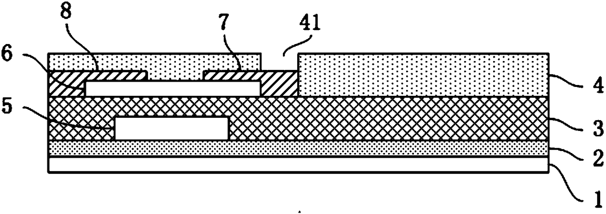
[0030] The invention provides a thin film transistor used in a display panel, such as Figure 3a As shown, the thin film transistor includes: a gate 5 and a gate insulating layer 3 located above the glass substrate 1 in the display panel, and the gate insulating layer 3 covers the gate 5; the gate 5 is located in the non-display area of ​​the display panel.

[0031] An active layer 6 is provided above the gate insulating layer 3 , and the active layer 6 is located above the gate 5 , and a source 7 and a drain 8 are also provided on the active layer 6 .

[0032] Among them, such as Figure 4 As shown, in the direction away from the glass substrate 1, the grid 5 sequentially includes a first non-metal layer 52 and a metal layer 51, the first non-metal layer 52 is one of Si layer, SiNx layer, SiOx layer, x> 1.

[0033] Further, the metal layer 51 includes a first metal layer 512 and a second metal layer 511 , and the first metal layer 512 is located between the second metal lay...


PUM

PropertyMeasurementUnit
thicknessaaaaaaaaaa
thicknessaaaaaaaaaa
thicknessaaaaaaaaaa

Abstract

The invention provides a thin film transistor used in a display panel and the display panel. The thin film transistor comprises a gate and a gate insulation layer, wherein the gate is arranged on a glass substrate in the display panel, the gate insulation layer covers the gate, the gate is arranged on a non-display region of the display panel, an active layer is arranged on the gate insulation layer and is arranged above the gate, the active layer is further provided with a source and a drain, and the gate sequentially comprises a first non-metal layer and a metal layer in a direction far awayfrom the glass substrate. By the thin film transistor, the influence of reflective light can be improved on the premise of no increase on cost of the display panel, the reflectivity is reduced, and the display quality is improved.

Description

technical field [0001] The invention relates to the field of display technology, in particular to a thin film transistor used in a display panel and the display panel. Background technique [0002] The structure diagram of AM (active) display device is as follows figure 1 As shown, the schematic diagram of the structure of the thin film transistor contained in it is shown in figure 2 shown. figure 1 with figure 2 The symbols 1', 2', 3', 4', 5', and 6' are glass substrates, insulating layers, a-Si layers (amorphous silicon layers), data lines, gate lines, and pixel electrodes, respectively. [0003] AM display devices include AM-OLED (OLED, organic light emitting diode) and AM-LCD (LCD, liquid crystal display) panels. [0004] The metal electrodes of thin film transistors in AM display devices generally use metals such as Cu, Al, Ag, Au, Mo, Cr or composite metal structures such as Mo and Cu, Mo and Al, Mo and Al, and Mo. However, no matter whether the previous single ...

Claims


Application Information

Patent Timeline
Patent Type & Authority Applications(China)
IPC IPC(8): H01L29/786H01L29/49H01L27/32G02F1/1368
CPCH01L29/4908H01L29/4966H01L29/786G02F1/1368H10K59/12
Inventor 樊勇
Owner HUIZHOU CHINA STAR OPTOELECTRONICS TECHNOLOGY CO LTD
Why Eureka
Try Eureka