
Nitride light emitting diode structure

A technology of light-emitting diodes and nitrides, which is applied in the direction of electrical components, circuits, semiconductor devices, etc., can solve the problems of reducing the internal quantum efficiency of LEDs and low internal quantum efficiency, and achieve the effect of improving internal quantum efficiency and increasing the probability of tunneling

Pending Publication Date: 2018-07-27
NANCHANG UNIV +1
View PDF6 Cites 3 Cited by
  • Summary
  • Abstract
  • Description
  • Claims
  • Application Information

AI Technical Summary

Problems solved by technology

However, due to the existence of a strong polarized electric field in the InGaN quantum well, the InGaN quantum well is affected by the "quantum confinement Stark effect", which leads to the energy band tilt of the InGaN quantum well, and the space separation of the hole and electron wave functions, thereby reducing the The internal quantum efficiency of LED, the thicker the GaN quantum barrier, the more serious the quantum confinement Stark effect, and the lower the internal quantum efficiency of LED

Method used


Image

  • Nitride light emitting diode structure
  • Nitride light emitting diode structure

Examples


Embodiment 1

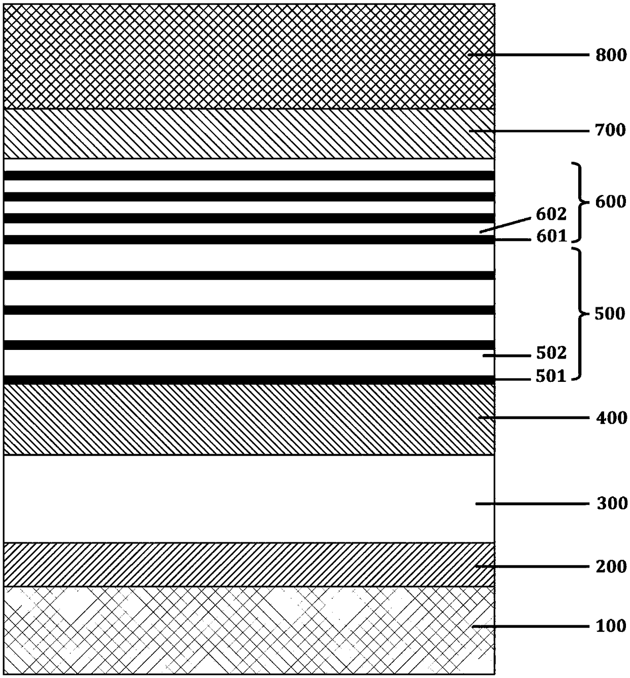
[0022] Such as figure 1 As shown, the substrate 100 is a silicon (Si) substrate, the buffer layer 200 is AlN, and the N-type layer 300 is Si-doped with a concentration of 2×10 18 ~5×10 18 cm -3 GaN, the preparation layer 400 is In with a thickness of 80nm-100nm 0.05 Ga 0.95 N single-layer structure; the first multi-quantum well layer 500 is 4 periods of In x Ga (1-x) N / GaN periodic structure, wherein the thickness of the GaN quantum barrier is 15nm; the second multi-quantum well layer 600 is 4 periods of In x Ga (1-x) N / GaN periodic structure, wherein the thickness of the GaN quantum barrier is 10nm; 19 cm -3 Al 0.2 Ga 0.8 N; P-type layer 800 is doped with Mg concentration 1×10 20 cm -3 GaN.

Embodiment 2

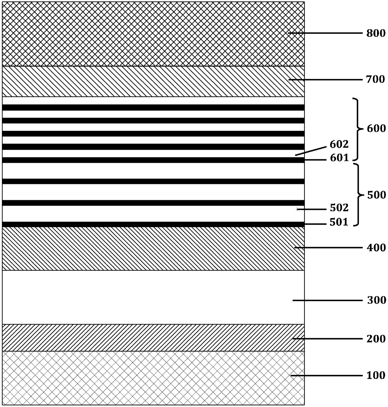
[0024] Such as figure 2 As shown, the substrate 100 is made of sapphire (Al 2 o 3 ) substrate, the buffer layer 200 is low-temperature GaN, and the N-type layer 300 is doped with Si concentration 5×10 18 ~1×10 19 cm -3 GaN; preparation layer 400 is In 0.05 Ga 0.95 N / GaN periodic structure, the number of periods is 20-30; the first multi-quantum well layer 500 is 3 periods of In x Ga (1-x) N / GaN periodic structure, wherein the thickness of the GaN quantum barrier is 10nm; the second multi-quantum well layer 600 is 5 periods of In x Ga (1-x)N / GaN periodic structure, wherein the thickness of the GaN quantum barrier is 7nm; 19 cm -3 Al 0.15 Ga 0.85 N; P-type layer 800 is Mg-doped concentration 5×10 19 cm -3 GaN.


PUM


Abstract

The invention provides a nitride light emitting diode structure. The structure comprises a substrate, the substrate is provided with a buffer layer, the buffer layer is provided with a N-type layer, apreparation layer, a first multiple quantum well layer, a second multiple quantum well layer, a P-type electron clocking layer and a P-type layer in sequence, and the first multiple quantum well layer comprises quantum wells of the first multiple quantum well layer and quantum barriers of the first multiple quantum well layer; the second multiple quantum well layer comprises quantum wells of thesecond multiple quantum well layer and quantum barriers of the second multiple quantum well layer; and the thickness of the quantum barriers of the first multiple quantum well layer is greater than that of the second multiple quantum well layer. According to the nitride light emitting diode structure, the thickness of the quantum barriers close to one side of the P-type layer is thinned, thereby effectively slowing down a 'quantum restriction stark effect' of light emitting wells close to one side of the P-type layer and improving the inner quantum efficiency of a light emitting diode.

Description

technical field [0001] The invention relates to semiconductor materials, in particular to a nitride light emitting diode structure. Background technique [0002] Light-emitting diodes (LEDs) have been widely concerned and researched for their remarkable characteristics of energy saving, environmental protection and high reliability. Today, as the energy crisis and environmental crisis are getting worse, many countries and regions have listed LED lighting technology as a national development strategy. After more than 20 years of research and hard work, LED epitaxial growth technology, LED chip manufacturing technology and LED packaging technology have all made great progress, making LEDs widely used in display screens, indicator lights, landscape lighting, automotive lights, general lighting, etc. field. [0003] The active layer of a nitride LED is generally an InGaN / GaN multi-quantum well barrier structure, where InGaN is a quantum well and GaN is a quantum barrier. The ...

Claims


Application Information

Patent Timeline
Patent Type & Authority Applications(China)
IPC IPC(8): H01L33/06H01L33/32H01L33/12H01L33/14
CPCH01L33/06H01L33/12H01L33/14H01L33/32
Inventor 刘军林莫春兰张建立王小兰郑畅达全知觉江风益
Owner NANCHANG UNIV
Learn More