DBR structure and LED chip provided with DBR structure

A technology of LED chip and layered structure, which is applied in the direction of electrical components, circuits, semiconductor devices, etc., can solve the problems of the influence of incident light reflectivity and the reduction of large-angle incident light reflectivity, etc., to reduce production costs, improve reflectivity, The effect of simplifying the manufacturing process

Inactive Publication Date: 2018-07-31
ENRAYTEK OPTOELECTRONICS
View PDF0 Cites 1 Cited by
  • Summary
  • Abstract
  • Description
  • Claims
  • Application Information

AI Technical Summary

Problems solved by technology

However, when the two center wavelengths are close to each other, the reflectivity of the DBR film to the incident light at a large angle will be greatly reduced. When the two center wavelengths are far apart, the reflectivity of the incident light at a small angle will be affected.

Method used


Image

  • DBR structure and LED chip provided with DBR structure

Examples


Embodiment Construction

[0017] The present invention will be further elaborated below by describing a preferred specific embodiment in detail in conjunction with the accompanying drawings.

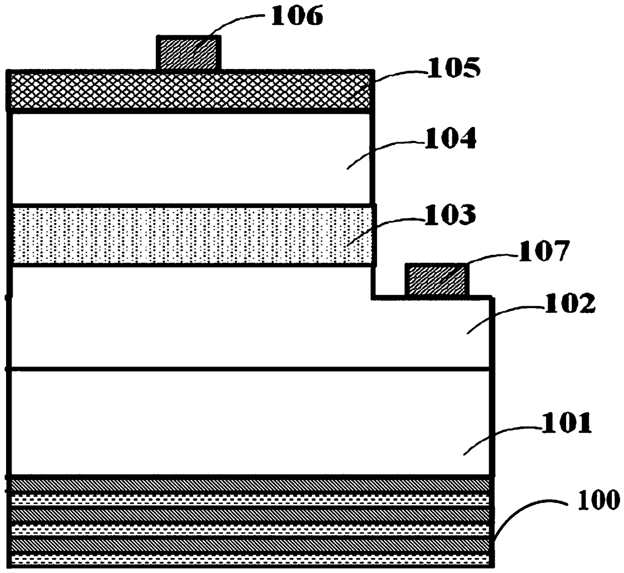
[0018] Such as figure 1 As shown, an LED chip with a DBR structure in the present invention includes: an epitaxial layer is formed by epitaxial growth on a sapphire substrate 101 of a wafer; Layer 102, light emitting layer 103 and P-type layer 104.

[0019] By means of photolithography or plasma gas etching, the P-type layer 104, light-emitting layer 103, and part of the N-type layer 102 are etched and removed at a distance from the edge of the epitaxial layer until the N-type layer is exposed. Layer 102, forming a step; the step serves as an N-type region of each LED chip. An N electrode 107 is fabricated on the steps of the exposed N-type layer 102, and a conductive layer 105 is formed on the surface of the P-type layer 104 by means of evaporation or metal sputtering. The P electrode 106 is formed on the con...


PUM


Abstract

The invention discloses a DBR structure and an LED chip provided with the DBR structure. At least three groups of film systems are included. The center wavelength of the first group of film systems islambda1. The center wavelength of the third group of film systems is lambda3. The center wavelength of the second group of film systems located between the first group of film systems and the third group of film systems is lambda2, wherein the lambda2 satisfies the following equation: lambda2=(lambda1+lambda3) / 2. The optical thickness d1 of the first group of film systems is equal to the opticalthickness d3 of the third group of film systems. The optical thickness d2 of the second group of film systems is (lambda2 / lambda1+lambda3 / lambda2) / 4 times the thickness of the third or first group offilm systems. In the invention, under the condition of guaranteeing small-angle incident light reflectivity, large-angle incident light reflectivity is increased and the brightness of the LED chip isgreatly increased too.

Description

technical field [0001] The invention relates to the technical field of light-emitting diode epitaxy, in particular to a DBR structure and an LED chip provided with the DBR structure. Background technique [0002] In recent years, high-brightness light-emitting diodes (LEDs) have the characteristics of low power consumption, high luminous efficiency, long life, small size and low cost. Therefore, it has a wide range of applications in lighting and optical fiber communication systems. [0003] In the prior art, in order to improve the luminous efficiency and luminous brightness of LEDs, methods such as flip-chip structures, transparent substrates, and inverted pyramid structures are used to improve the brightness of LEDs, but these methods still have problems such as complex processes and high costs. [0004] In the prior art, a Bragg reflective layer (DBR) is also used to increase the brightness of the chip including the light-emitting diode. The DBR film in a common LED is ...

Claims


Application Information

Patent Timeline
Patent Type & Authority Applications(China)
IPC IPC(8): H01L33/46
CPCH01L33/46H01L2933/0025
Inventor 赵龙王亚洲
Owner ENRAYTEK OPTOELECTRONICS
Why Eureka
Try Eureka