Double-sided light emitting diode (LED) light source structure based on COB packaging structure

A LED light source and double-sided light-emitting technology, which is applied in the direction of electrical components, electric solid devices, circuits, etc., can solve the problems of affecting the light efficiency and stability of LED light sources, affecting the service life of LED light sources, and reducing light efficiency, so as to prevent high Voltage electrostatic breakdown, improve safety and stability, and improve light efficiency

Pending Publication Date: 2018-08-03
广州东有电子科技有限公司
View PDF0 Cites 0 Cited by
  • Summary
  • Abstract
  • Description
  • Claims
  • Application Information

AI Technical Summary

Problems solved by technology

It mainly has the following disadvantages: on the one hand, since the mirror metal substrate or the ordinary ceramic substrate are non-transparent substrates, the traditional LED light source based on the COB package structure can only form single-sided light emission, which not only has low light efficiency, but also Seriously affect the service life of the LED light source; on the other hand, since the front of the mirror metal substrate or ordinary ceramic substrate is usually dotted with fluorescent glue, the fluorescent powder mixed with transparent colloid material is directly coated on the LED chip, while the ordinary LED chip The photoelectric conversion efficiency of LED is generally 30% to 50%, and it will generate a lot of heat when it emits light, so that the temperature around the LED chip will reach 150°C to 200°C, and the long-term work of the phosphor at high temperature will cause very Serious attenuation affects the light efficiency and stability of the LED light source, and the yellowing of silica gel under high temperature for a long time leads to a decrease in light efficiency

Method used


Image

  • Double-sided light emitting diode (LED) light source structure based on COB packaging structure
  • Double-sided light emitting diode (LED) light source structure based on COB packaging structure
  • Double-sided light emitting diode (LED) light source structure based on COB packaging structure

Examples


Embodiment Construction

[0021] The present invention will be further elaborated below in conjunction with accompanying drawing, wherein, the direction of the present invention is with figure 1 as standard.

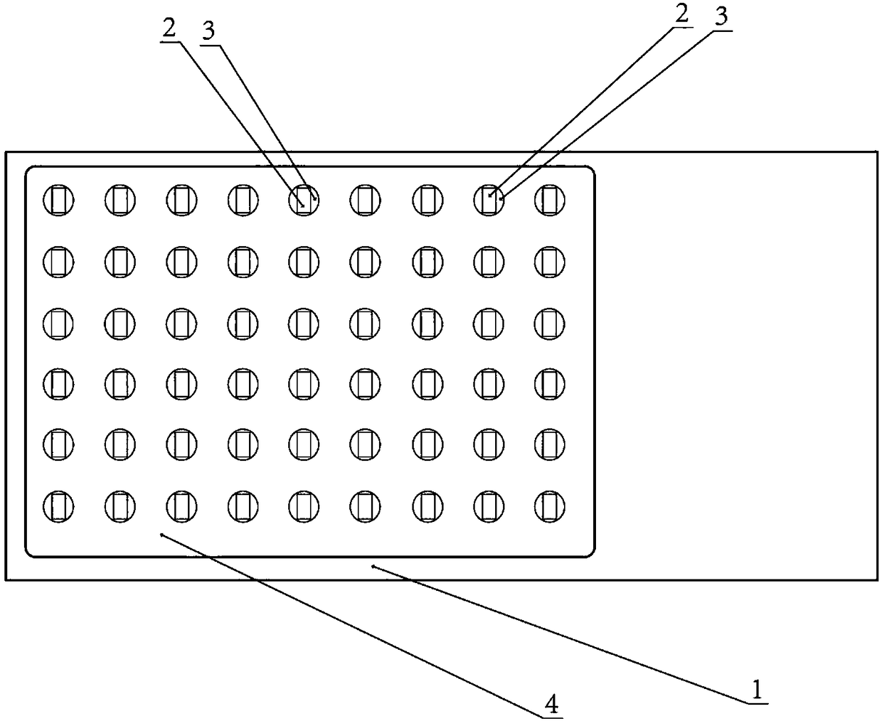
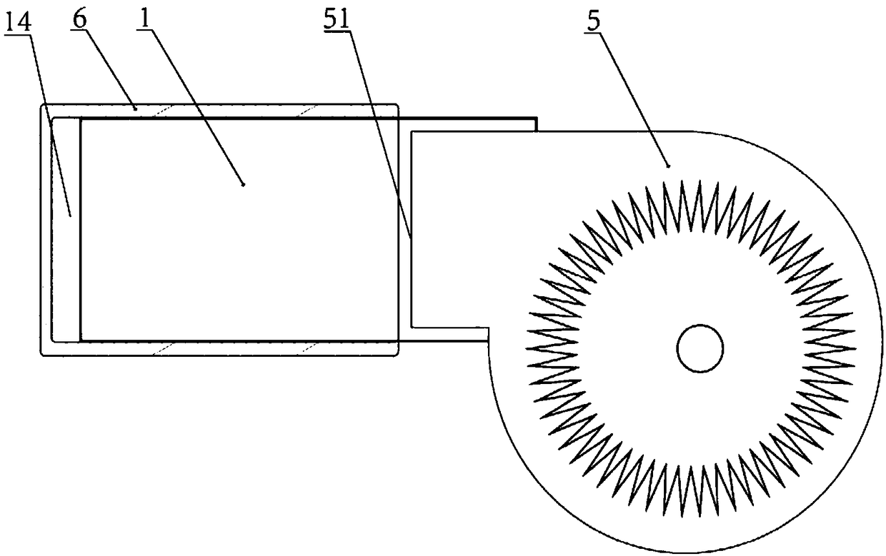
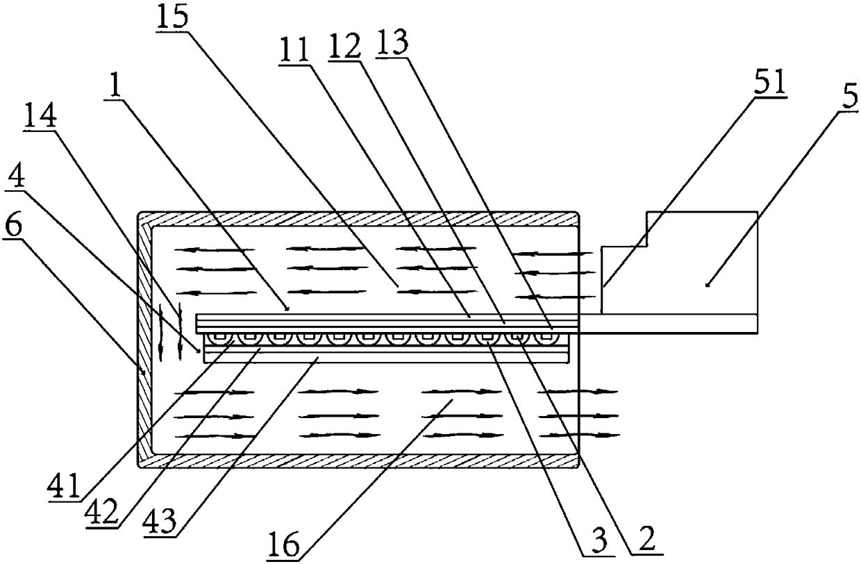
[0022] Such as Figure 1 to Figure 4 As shown, the double-sided light-emitting LED light source structure based on the COB packaging structure of the present invention includes a multilayer ceramic substrate 1, an LED chip array 2 arranged on the multilayer ceramic substrate 1, a silver glue conductive circuit, and a light-transmitting ceramic lens 3 , fluorescent adhesive layer 4, heat dissipation device 5 and heat dissipation lampshade 6, wherein:

[0023] The multilayer ceramic substrate 1 is a light-transmitting ceramic layer substrate made of nano-materials in the prior art. The multilayer ceramic substrate 1 includes a light-transmitting and pressure-resistant ceramic layer 11, a light-transmitting high-thermal-conductivity ceramic layer 12 and a light-transmitting fluorescent ceramic laye...


PUM

PropertyMeasurementUnit
radiusaaaaaaaaaa
wavelengthaaaaaaaaaa
refractive indexaaaaaaaaaa

Abstract

The invention discloses a double-side LED light source structure based on a COB packaging structure. The double-side LED light source structure based on a COB packaging structure comprises a multilayer ceramic substrate, a LED chip array, a silver glue conductive circuit and a fluorescent adhesive layer are arranged on the multilayer ceramic substrate, the multilayer ceramic substrate is a transparent ceramic substrate, the silver glue conductive circuit is arranged on the front surface of the multilayer ceramic substrate; the LED chip array comprises a plurality of LED chips which are uniformly arranged at intervals, and the LED chips are electrically connected with the silver glue conductive circuit; the fluorescent glue layer comprises a wafer protection glue layer, a thermal insulationlayer and a fluorescent layer, wherein the wafer protection glue layer cover is arranged on the LED chip, the thermal insulation layer is arranged on the wafer protection glue layer, and the fluorescent layer is arranged on the thermal insulation layer. The double-side LED light source structure based on a COB packaging structure can achieve double-sided give out light to improve the lighting effect, has the advantages of good heat dissipation performance, high energy efficiency, high luminous flux and high thermal stability, and can avoid the attenuation of the fluorescent powder or the failure of the light source at high temperature.

Description

technical field [0001] The invention relates to an LED light source structure, in particular to a double-sided LED light source structure based on a COB packaging structure. Background technique [0002] With the rapid development of LED technology, its luminous efficiency continues to increase, and the price continues to decline. The preparation technology of white light LEDs has become increasingly mature. LED light sources have many advantages such as high luminous flux, long life, small structure, safety, high efficiency, and energy saving. Become the best light source choice to replace traditional lighting sources. [0003] The traditional LED light source based on the COB packaging structure is usually to directly bond the LED chips on the mirror metal substrate with high light reflection rate or on the ordinary ceramic substrate, and then connect the LED chips in series and parallel through methods such as gold wires, and finally Dispense fluorescent glue above the L...

Claims


Application Information

Patent Timeline
Patent Type & Authority Applications(China)
IPC IPC(8): H01L25/075H01L33/48H01L33/64H01L33/52H01L33/58H01L33/62
CPCH01L25/0753H01L33/48H01L33/52H01L33/58H01L33/62H01L33/64
Inventor 黎兆早赖志文翟永刚
Owner 广州东有电子科技有限公司
Why Eureka
Try Eureka