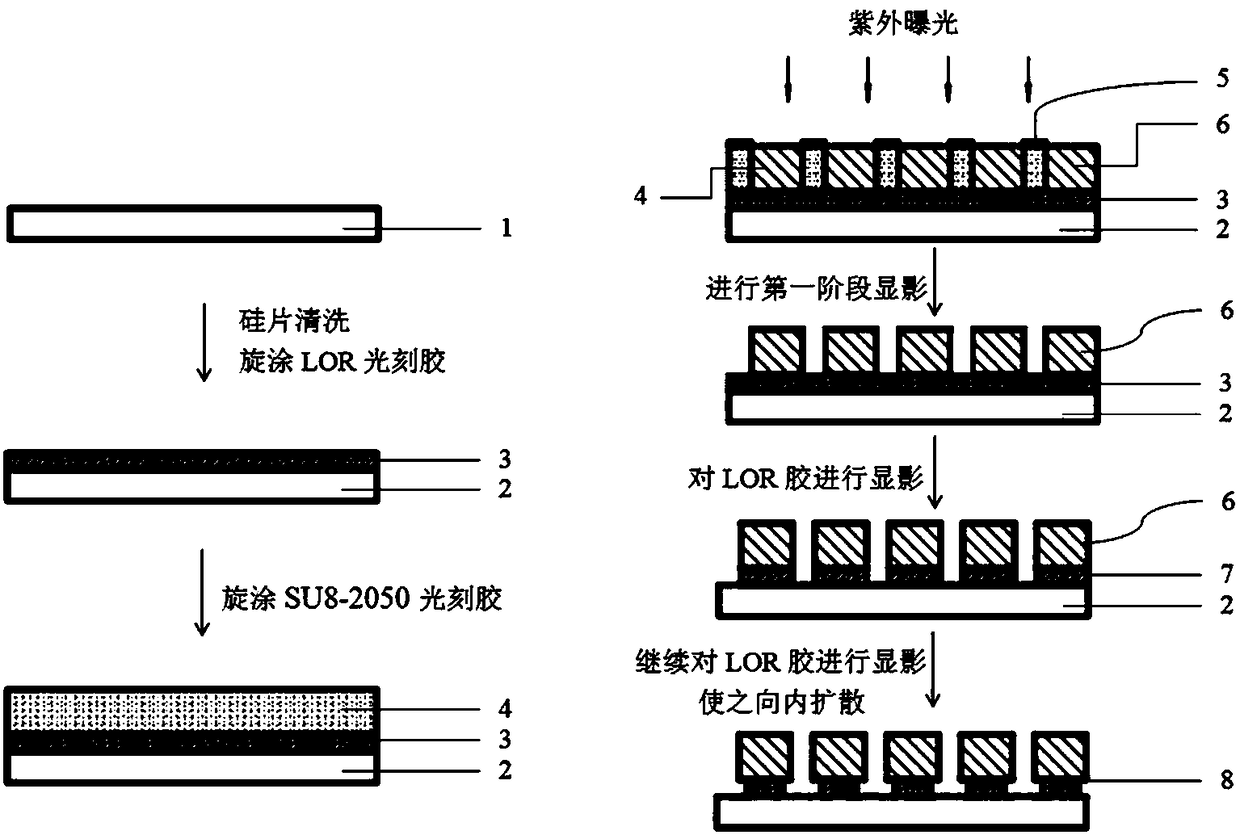
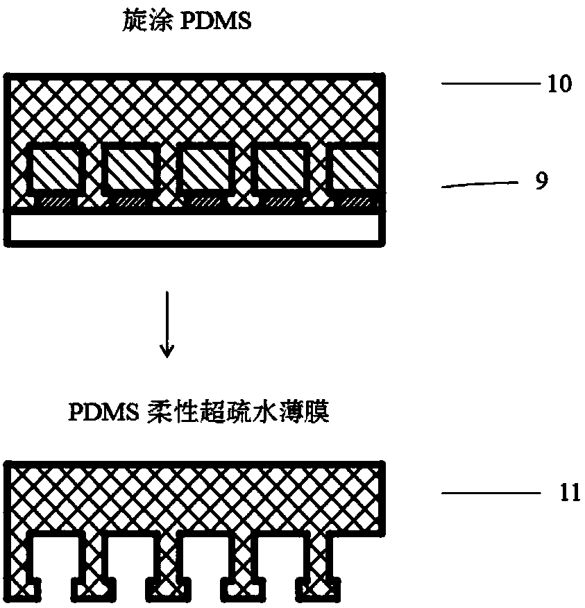
Method for manufacturing PDMS flexible super-hydrophobic film
A production method and super-hydrophobic technology, applied in the manufacture of microstructure devices, techniques for producing decorative surface effects, decorative arts, etc., can solve the problems of development, expensive equipment, and high cost, and achieve reduced production costs and good hydrophobic properties , the effect of low surface energy
- Summary
- Abstract
- Description
- Claims
- Application Information
AI Technical Summary
Problems solved by technology
Method used
Image
Examples
Embodiment 1
[0030] Example 1. Preparation of a PDMS flexible superhydrophobic film with an Under cut structure size of 10 μm and a thickness of 100-150 μm
[0032] Use acetone, isopropanol and deionized water in sequence to ultrasonically clean the silicon wafer, and then dry it to obtain a clean silicon wafer;
[0033] b. Preparation of single-layer photoresist substrate
[0034] Spin-coat LOR photoresist on the surface of a clean silicon wafer with a spin-coating thickness of 5 μm, then bake at 200°C for 10 minutes, and then cool to room temperature to form a single-layer photoresist substrate; wherein, the initial spin-coating speed is 500rpm and lasts 10s , and then accelerate to 1500rpm for 30s;
[0035] c. Preparation of double-layer photoresist substrate
[0036] Spin-coat SU8-2050 photoresist on the surface of a single-layer photoresist substrate with a spin-coating thickness of 60 μm, then bake at 65°C for 3 minutes, then bake at 90°C for 10 min...
Embodiment 2
[0047] Example 2. Preparation of a PDMS flexible superhydrophobic film with an Under cut structure size of 50 μm
[0048] a. Clean silicon wafer
[0049] Silicon wafers were ultrasonically cleaned with acetone, isopropanol and deionized water in sequence, and then dried to obtain clean silicon wafers;
[0050] b. Preparation of single-layer photoresist substrate
[0051] Spin-coat LOR photoresist on the surface of a clean silicon wafer with a spin-coating thickness of 3 μm, then bake at 170°C for 10 minutes, and then cool to room temperature to form a single-layer photoresist substrate; where the initial spin-coating speed is 500rpm and lasts for 10s , and then accelerate to 2000rpm for 30s;
[0052] c. Preparation of double-layer photoresist substrate
[0053] Spin-coat SU8-2050 photoresist on the surface of a single-layer photoresist substrate with a spin-coating thickness of 40 μm, then bake at 65°C for 3 minutes, then bake at 90°C for 10 minutes, and finally cool to roo...
PUM
| Property | Measurement | Unit |
|---|---|---|
| thickness | aaaaa | aaaaa |
Abstract
Description
Claims
Application Information

