

Leveling method of flexible thin film material and application of leveling method
A flexible thin-film material and processing method technology, which is applied in the fields of climate sustainability, photovoltaic power generation, electrical components, etc. damage and other problems, to achieve the effect of significant flattening effect, low cost and smooth surface
- Summary
- Abstract
- Description
- Claims
- Application Information
AI Technical Summary
Problems solved by technology
Method used
Image

Examples
Embodiment Construction
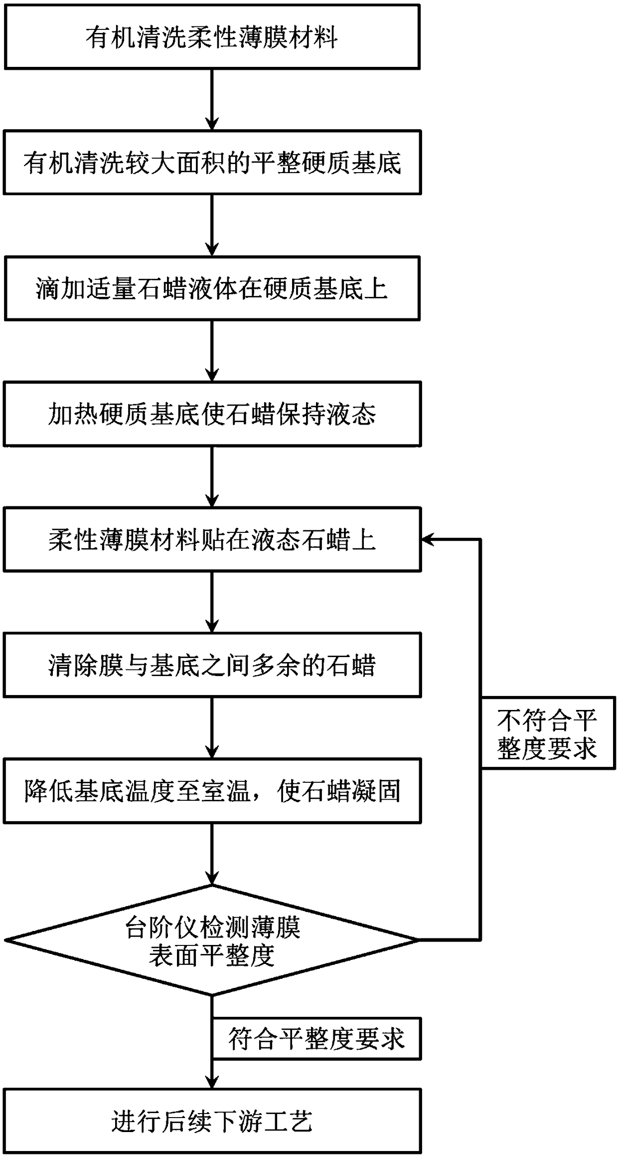
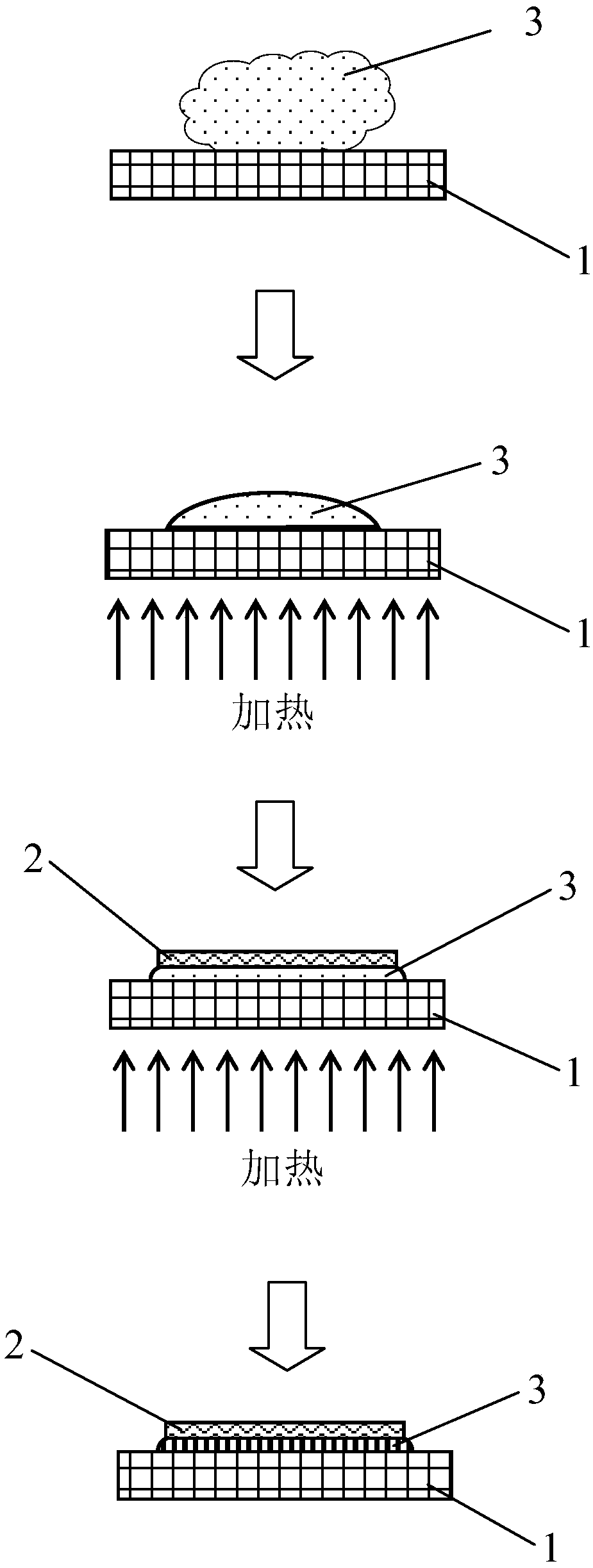
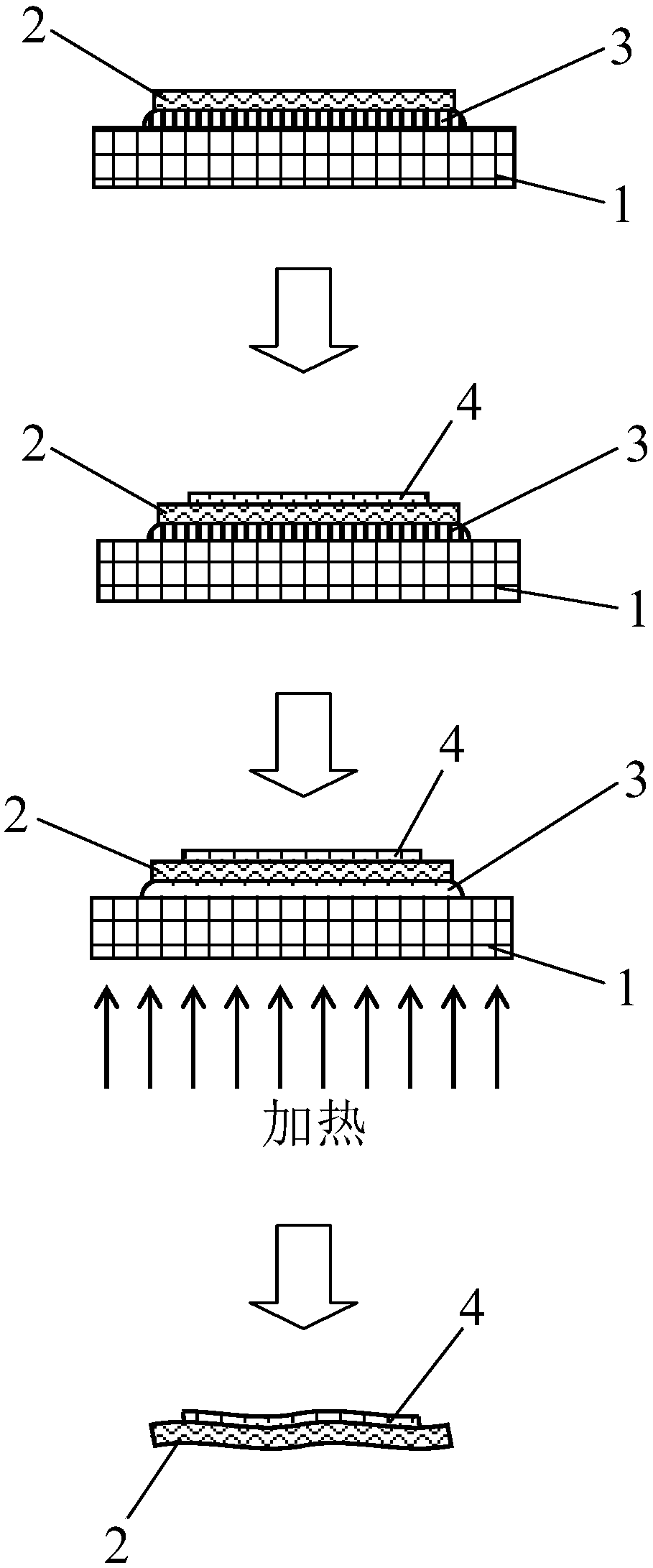
[0046] See figure 1 with figure 2 , The flattening treatment method of the flexible film material of the present invention includes the following steps:
[0047] S1: Cleaning the hard substrate 1 and the flexible film material 2 to remove particulate impurities and organic matter on the surface, specifically including the following steps:
[0048] S11: Choose any one of glass, quartz wafer, polished silicon wafer, ruby, ceramic, etc., and cut into a 2cm×2cm square substrate as the hard substrate 1. Then, put the cut hard substrate 1 in acetone for ultrasonic cleaning for 10 minutes to remove organic impurities on the surface, then put it in isopropanol for ultrasonic cleaning for 5 minutes to remove residual acetone on the surface, and then put it in absolute ethanol Ultrasonic cleaning for 5 minutes to remove the residual isopropanol on the surface, and then soak and clean with deionized water for 10 times to remove the residual ethanol on the surface, and then put it in a 60℃ ov...
PUM
| Property | Measurement | Unit |
|---|---|---|
| melting point | aaaaa | aaaaa |
| boiling point | aaaaa | aaaaa |
Abstract
Description
Claims
Application Information