
Method for rapidly producing surface enhanced Raman active substrate

A surface-enhanced Raman and active substrate technology, applied in the field of analytical chemistry and nanometers, can solve the problems of high cost, cumbersome operation, and long time consumption, and achieve the effect of rapid detection

Inactive Publication Date: 2018-08-17
FUZHOU UNIV
View PDF3 Cites 8 Cited by
  • Summary
  • Abstract
  • Description
  • Claims
  • Application Information

AI Technical Summary

Problems solved by technology

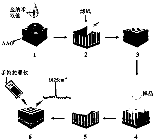
[0005] The present invention aims at the problems of time-consuming, high cost, cumbersome operation, and unsuitable for large-scale promotion in the preparation of surface-enhanced Raman active substrates, and proposes a method for rapidly preparing surface-enhanced Raman active substrates, which utilizes porous anodic oxidation Aluminum (AAO) is used as a template, drop the gold nano-bicone solution on the surface of AAO, absorb the excess gold nano-bicone solution on the surface with filter paper, then the gold nano-bicone in the hole will be self-assembled and stay in the AAO hole

Method used


Image

  • Method for rapidly producing surface enhanced Raman active substrate
  • Method for rapidly producing surface enhanced Raman active substrate
  • Method for rapidly producing surface enhanced Raman active substrate

Examples


Embodiment 1

[0031] Example 1: Construction of Au NBPS-AAO surface-enhanced Raman substrate.

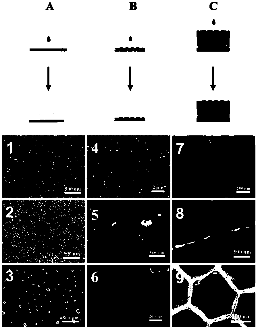
[0032] First use a size of 3.0 × 3.0 mm 2 The left and right porous anodized aluminum (pore diameter 300 nm, pore spacing 450 nm, pore depth 5 μm) was used as a template, and 10 μL of 1.2 × 10 −7 The gold nanobiconic solution of M was added dropwise on the surface of the AAO template, followed by a 2.0 × 2.0 cm 2 The filter paper absorbs the excess gold nanobicone solution on the surface of the AAO template. At this time, most of the gold nanobicone solution in the channel will remain inside. After 10 s of natural drying, the gold nanobicone will remain in each nanopore In the channel, the Au NBPs-AAO surface-enhanced Raman substrate was obtained immediately. Related operating principles such as figure 1 As shown, the Au NBPs-AAO surface-enhanced Raman substrate is characterized as figure 2 shown.

Embodiment 2

[0033] Example 2: Comparison of surface-enhanced Raman substrates prepared by different templates.

[0034] On the surface of the silicon wafer, the surface of porous anodized aluminum oxide Ⅰ (pore diameter 400 nm, pore spacing 450 nm, pore depth 100 nm), porous anodic aluminum oxide Ⅱ surface (pore diameter 300 nm, pore spacing 450 nm, pore depth 5 μm) was added dropwise 10 μL 1.2 × 10 −7 M gold nanobipyramidal solution, followed by a solution with a size of 2.0 × 2.0 cm 2 filter paper, absorb the excess gold nano-bicone solution on the surface of three different templates, and after standing for 10 seconds, three different surface-enhanced Raman active substrates can be obtained. 10 μL of rhodamine 6 G solution was added dropwise on the surface of the above three different surface-enhanced Raman active substrates, and then a 2.0 × 2.0 cm 2 The filter paper was used to absorb the excess rhodamine 6 G solution on the surface of three different surface-enhanced Raman active...


PUM

PropertyMeasurementUnit
Apertureaaaaaaaaaa
Hole depthaaaaaaaaaa
Hole spacingaaaaaaaaaa

Abstract

The invention discloses a method for rapidly producing a surface enhanced Raman active substrate. The Au NBPs-AAO surface enhanced Raman active substrate is constructed by self-assembling a gold nano-bipyramid used as a precious metal nanoparticle in the nano-pores of porous anodised aluminum oxide (AAO) used as a template. The method allows the surface enhanced Raman active substrate to be produced within 10 s, and the detection of rhodamine 6G by using the surface enhanced Raman active substrate produced through method can be completed within 10 s with handheld Raman as a detection tool.

Description

technical field [0001] The invention relates to a method for rapidly preparing a surface-enhanced Raman active substrate, which belongs to the fields of analytical chemistry and nanotechnology. Background technique [0002] Analytical methods based on surface-enhanced Raman scattering (SERS) have been extensively studied over the past few decades because it provides the target's fingerprint signal and ultrasensitivity to the signal response. However, the application of surface-enhanced Raman scattering to sample detection still faces some key problems. For example, there are higher requirements for improving signal strength, reducing background noise, and reducing preprocessing time. To overcome these obstacles, researchers have developed a series of nanoparticles and fabrication methods to obtain more efficient surface-enhanced Raman active substrates. Based on the manufacturing method, the present invention proposes a method for rapidly preparing a surface-enhanced Raman...

Claims


Application Information

Patent Timeline
IPC IPC(8): G01N21/65B82Y30/00B82Y40/00
CPCB82Y30/00B82Y40/00G01N21/658
Inventor 郭隆华林丙永邱彬林振宇陈国南
Owner FUZHOU UNIV
Learn More