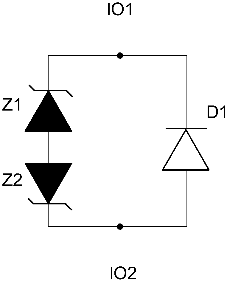
Bidirectional TVS device with anti-parallel diode and preparation method thereof
A technology of diodes and manufacturing methods, applied in semiconductor/solid-state device manufacturing, semiconductor devices, electrical components, etc., can solve problems such as unsatisfactory, one-way one TVS is difficult to meet the diversification of two-way different voltage gears, etc., to improve the response. The effect of speed, power consumption and cooling advantages, excellent performance
- Summary
- Abstract
- Description
- Claims
- Application Information
AI Technical Summary
Problems solved by technology
Method used
Image
Examples
Embodiment 1
[0049] The structure of the bidirectional TVS device with the antiparallel diode of the present embodiment is as follows Figure 14 As shown, it includes a P-type silicon substrate 22, the front of the P-type silicon substrate is provided with N-type doped regions 31 and P-type doped regions 32, and the back of the P-type silicon substrate is provided with N-type doped regions. Region 31 and P-type doped region 32, the N-type doped region on the front side of the P-type silicon substrate is made of metal 41, and the N-type doped region and P-type doped region on the back side of the P-type silicon substrate are made The interconnection metal 41 is drawn out; the distance between the N-type doped region and the P-type doped region on the back of the P-type silicon substrate is greater than zero.
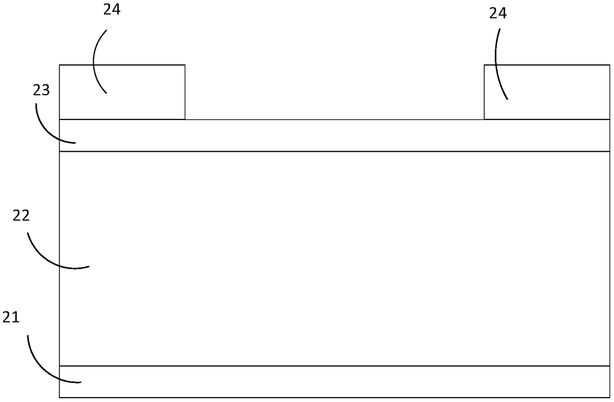
[0050] Its preparation process is as Figure 2-14 Shown:
[0051] Step (1): growing an oxide layer 21 and an oxide layer 23 simultaneously on the front and back sides of the P-type ...
Embodiment 2
[0063] Such as Figure 15 As shown, the structure of the bidirectional TVS device with anti-parallel diodes in this embodiment differs from that in Embodiment 1 in that the distance between the N-type doped region and the P-type doped region on the back is zero. Its preparation process is identical with embodiment 1.
Embodiment 3
[0065] Such as Figure 16 As shown, the structure of the bidirectional TVS device with anti-parallel diodes in this embodiment is different from Embodiment 1 in that: the N-type doped region on the back is on the outside, and the P-type doped region is on the inside, which is opposite to Embodiment 1. Its preparation process is also basically the same as that of Example 1, the difference is only in the adjustment of the positions of the N-type doped regions on the front and back sides during preparation.
PUM
| Property | Measurement | Unit |
|---|---|---|
| Resistivity | aaaaa | aaaaa |
Abstract
Description
Claims
Application Information


