Super-junction device and manufacturing method thereof

A technology of superjunction device and manufacturing method, which is applied in semiconductor/solid-state device manufacturing, semiconductor devices, electrical components, etc., and can solve problems such as poor softness factor

Active Publication Date: 2018-08-21
SHENZHEN SANRISE TECH CO LTD
View PDF4 Cites 3 Cited by
  • Summary
  • Abstract
  • Description
  • Claims
  • Application Information

AI Technical Summary

Problems solved by technology

However, since the P+ contact region in the P-type ring in the transition region is also very dense, the ability to collect holes under the forward Vds is very strong, so the process of the body diode of the device from normal c

Method used


Image

  • Super-junction device and manufacturing method thereof
  • Super-junction device and manufacturing method thereof
  • Super-junction device and manufacturing method thereof

Examples


no. 1 example approach

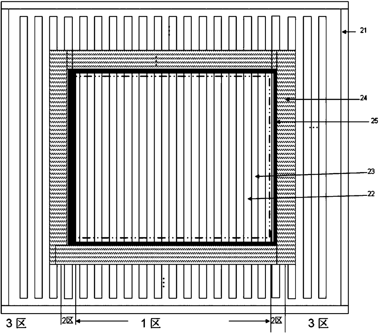
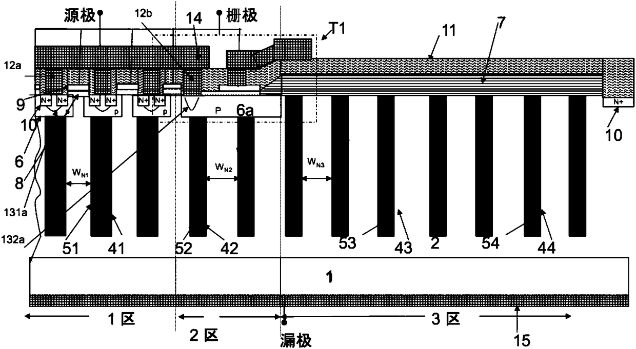
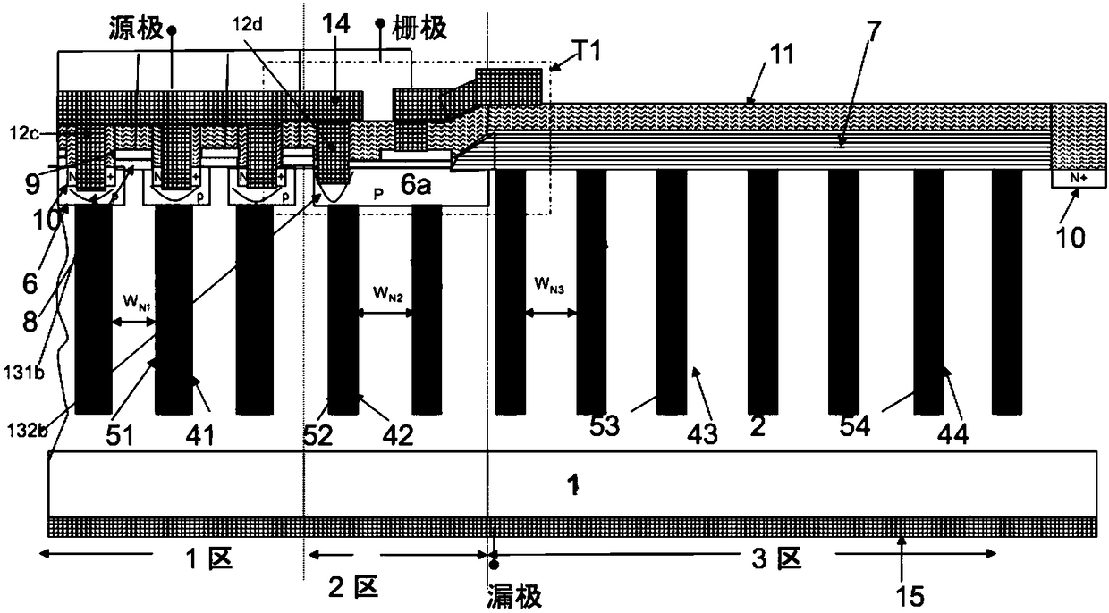
[0118] The manufacturing method of the super junction device of the first embodiment of the present invention is used to manufacture such Figure 4 The superjunction device of the first embodiment of the present invention is shown as an example for description, such as Figure 8A to Figure 8H Shown is a schematic cross-sectional view of the device in each step of the method for manufacturing a superjunction device according to the first embodiment of the present invention; in the method for manufacturing a superjunction device according to an embodiment of the present invention, the middle area of ​​the superjunction device is the charge flow area, namely zone 1, The terminal zone, namely zone 3, surrounds the periphery of the charge flow zone, and the transition zone, zone 2 is located between the charge flow zone and the terminal zone; the structure of the top view of the super junction device can also be referred to figure 1 Shown. The method of the first embodiment of the pre...


PUM


Abstract

The invention discloses a super-junction device, which is characterized in that a protective epoxy film exposes a charge flow region, completely covers a transition region and completely or mostly covers a terminal region, a second contact hole at the top of a P-type ring of the transition region is enabled to penetrate deeper than a first contact hole at the top of a P-type well of the charge flow region by the thickness of one protective epoxy film, and thus the junction depth of a second P+ contact region at the bottom of the second contact hole is enabled to be less than the junction depthof a first P+ contact region at the bottom of the first contact hole, so that the distance between a hole collected by the P-type ring to the second P+ contact region, and a softness factor of reverse recovery of a body diode of the device is increased. The invention further discloses a manufacturing method of the super-junction device. According to the invention, the reverse recovery characteristics of device can be improved, and the avalanche tolerance of the device is enhanced at the same time.

Description

Technical field [0001] The present invention relates to a method for manufacturing a semiconductor integrated circuit, in particular to a method for manufacturing a superjunction device. Background technique [0002] The super junction structure is a structure composed of alternately arranged N-type pillars and P-type pillars. If a super junction structure is used to replace the N-type drift region in a vertical double-diffused metal-oxide-semiconductor (VDMOS) device, a conduction path is provided through the N-type pillar in the conduction state. The P-type pillar does not provide a conduction path; in the off state, the PN pillar jointly bears the reverse bias voltage to form a Superjunction Metal-Oxide-Semiconductor Field-Effect Transistor (MOSFET). Super-junction MOSFET can greatly reduce the on-resistance of the device by using a low-resistivity epitaxial layer when the reverse breakdown voltage is the same as that of the traditional VDMOS device. [0003] In the existing s...

Claims


Application Information

Patent Timeline
IPC IPC(8): H01L29/06H01L21/336H01L29/78
CPCH01L29/0611H01L29/0615H01L29/0684H01L29/66477H01L29/78
Inventor 肖胜安曾大杰李东升
Owner SHENZHEN SANRISE TECH CO LTD
Why Eureka
Try Eureka