A Surface Mount Type Semiconductor Resistance Bridge Package Structure

A technology of packaging structure and resistance bridge, which is applied in the direction of semiconductor devices, semiconductor/solid-state device components, resistor shells/packaging shells/potting, etc. Consistency is poor and other problems, to achieve the effect of simple structure, fewer packaging process steps, and low interconnection resistance

Active Publication Date: 2020-10-30
JACAL ELECTRONICS WUXI
View PDF5 Cites 0 Cited by
  • Summary
  • Abstract
  • Description
  • Claims
  • Application Information

AI Technical Summary

Problems solved by technology

[0002] Existing resistor bridge packages usually install semiconductor resistor chips in the cavities of metal or ceramic bases (such as TO-shaped metal shells, pin pins, or surface-mounted ceramic bases, etc.), and use metal wires (such as gold wires / Gold strip or aluminum wire / aluminum strip, etc.) to interconnect the lead-out pad of the chip with the outer pin of the base, and then wrap the interconnection wire with insulating glue (including the chip bonding pad), the resistance of the semiconductor resistor chip The bridge area is exposed, or chip bonding, wire bonding, and encapsulation are performed on the printed circuit board (PCB). These all have many steps in the packaging process and large package size. The packaging is carried out one by one, and the packaging efficiency is low. , high packaging cost, and poor dimensional consistency after packaging, it cannot meet the requirements of automatic placement process

Method used


Image

  • A Surface Mount Type Semiconductor Resistance Bridge Package Structure
  • A Surface Mount Type Semiconductor Resistance Bridge Package Structure
  • A Surface Mount Type Semiconductor Resistance Bridge Package Structure

Examples


Embodiment

[0025] Embodiment: a kind of size is 2.00mm * 1.20mm * 0.50mm (1206 type) surface mounted semiconductor resistance bridge packaging structure:

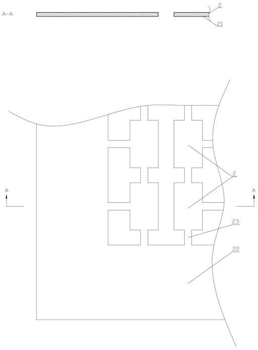
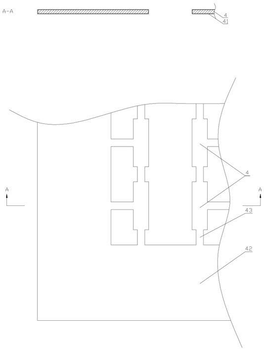
[0026] First, the metal electrode 2 and the metal electrode 4 are stamped or etched using a 100 μm thick C194 copper foil plated with (8±4) μm tin on the surface; the size of the metal electrode 2 is 1.25mm×0.80mm, such as figure 1 ; The size of the metal electrode 4 is 1.25mm × 0.40mm, such as image 3 ;

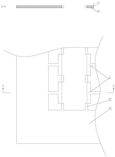
[0027] The metal electrode 3 is stamped or etched with a 300 μm thick C194 copper foil plated with (8±4) μm tin on the surface, and the size of the metal electrode 2 is 1.25mm×0.30mm, such as figure 2 .

[0028] Next, the middle layer metal electrode 3 is aligned and stacked on the bottom metal electrode 4, and a 300 μm thick 1.30mm×1.25mm semiconductor resistance bridge chip is loaded into the middle layer metal electrode 3, and then the top layer metal electrode 2 is aligned and stacked on it, and then Use a pressurized heat ...


PUM


Abstract

The invention discloses a surface mounting type semiconductor resistance bridge encapsulation structure. The encapsulation structure comprises a semiconductor resistance bridge chip, three layers of metal electrodes and an insulating glue layer; two leading end bonding pads of the semiconductor resistance bridge chip respectively have a solder plating coating layer; and every metal electrode has asolder plating coating layer. The leading end bonding pads of the semiconductor resistance bridge chip and the top metal electrode are thermocompression-bonded through the solder plating coating layers, the top metal electrode and the top metal electrode are thermocompression-bonded through the solder plating coating layers, and the middle metal electrode and the bottom metal electrode are thermocompression-bonded through the solder plating coating layers; and the semiconductor resistance bridge chip and the bottom metal electrode are bond-reinforced through epoxy and other insulating glues.The encapsulation structure uses the molded metal plate thermocompression-bonded structure with three solder plating coating layers to substitute substrate and chip bonding, metal leading wire bondingand encapsulation structure in the semiconductor resistance bridge, so the encapsulation structure has the advantages of simple structure, low encapsulation interconnection resistance, thinness in encapsulation, few encapsulation process steps, small device investment, and is suitable for thin and standardized surface mounting, low-cost and high-reliability requirements of the semiconductor resistance bridges in automobile airbags, automobile emergency hammers and digital electronic detonators.

Description

technical field [0001] The invention relates to the technical field of electronic packaging, in particular to a semiconductor resistance bridge packaging structure. Background technique [0002] Existing resistor bridge packages usually install semiconductor resistor chips in the cavities of metal or ceramic bases (such as TO-shaped metal shells, pin pins, or surface-mounted ceramic bases, etc.), and use metal wires (such as gold wires / Gold strip or aluminum wire / aluminum strip, etc.) to interconnect the lead-out pad of the chip with the outer pin of the base, and then wrap the interconnection wire with insulating glue (including the chip bonding pad), the resistance of the semiconductor resistor chip The bridge area is exposed, or chip bonding, wire bonding, and encapsulation are performed on the printed circuit board (PCB). These all have many steps in the packaging process and large package size. The packaging is carried out one by one, and the packaging efficiency is lo...

Claims


Application Information

Patent Timeline
Patent Type & Authority Patents(China)
IPC IPC(8): H01C1/02H01C1/032H01C1/14H01L23/48H01L23/64
CPCH01C1/02H01C1/032H01C1/14H01L23/485H01L23/647
Inventor 马国荣丁隽李保云
Owner JACAL ELECTRONICS WUXI
Why Eureka
Try Eureka