
An Out-of-Band Selectively Tunable Millimeter Wave Filter

A millimeter-wave, selective technology, applied in waveguide-type devices, circuits, electrical components, etc., can solve the problems of large filter volume, high manufacturing cost, and difficult multi-chip interconnection integration, etc. The effect of low loss and excellent out-of-band rejection

Active Publication Date: 2019-09-13
昆山鸿永微波科技有限公司
View PDF5 Cites 0 Cited by
  • Summary
  • Abstract
  • Description
  • Claims
  • Application Information

AI Technical Summary

Problems solved by technology

Traditional cavity and LC filters are bulky, expensive to manufacture, and difficult to integrate with multi-chip interconnects.

Method used


Image

  • An Out-of-Band Selectively Tunable Millimeter Wave Filter
  • An Out-of-Band Selectively Tunable Millimeter Wave Filter
  • An Out-of-Band Selectively Tunable Millimeter Wave Filter

Examples


Embodiment Construction

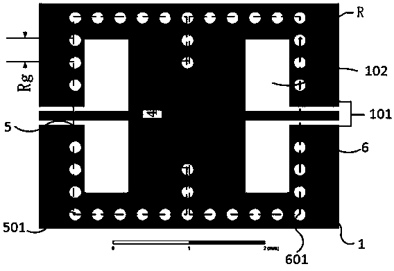
[0025] The following will clearly and completely describe the technical solutions in the embodiments of the present invention. Obviously, the described embodiments are only some of the embodiments of the present invention, rather than all the embodiments. Based on the embodiments of the present invention, all other embodiments obtained by persons of ordinary skill in the art without making creative efforts belong to the protection scope of the present invention.

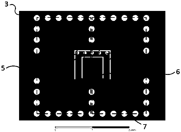
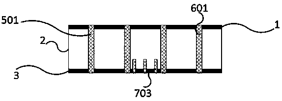
[0026] see Figure 1~Figure 6 , the embodiment of the present invention includes:

[0027] The upper metal layer 1 is formed by depositing electroplating metal on the upper surface of the high resistance silicon dielectric layer 2, and the bottom metal layer 3 is formed by depositing electroplating metal on the lower surface of the high resistance silicon dielectric layer 2. The gold plating thickness is 10um, and the material is gold, high resistance silicon The dielectric layer 2 is made of 500um thick high-resist...


PUM


Abstract

The present invention discloses a millimeter wave filter with adjustable out-of-band selectivity. The millimeter wave filter comprises a silicon cavity resonance unit 5, a silicon cavity resonance unit 6 and a selectivity adjustable unit 7. The silicon cavity resonance unit 5 and the silicon cavity resonance unit 6 are respectively formed by array arrangement of deep silicon etching through holes501 and 601 penetrating an upper metal layer 1, a high-resistance silicon dielectric layer 2 and a bottom metal layer 3, the selectivity adjustable unit 7 is formed by a half-wavelength defect ring resonance unit 701 and a half-wavelength defect ring resonance unit 702 which are etched on the bottom metal layer 3 and shallow silicon etching through holes 703 penetrating part of the high-resistancesilicon dielectric layer 2 and the bottom metal layer 3, the selectivity adjustable unit 7 employs a circuit structure, a through hole layout and a process layer design to allow high-frequency and low-frequency out-of-band rejection of the millimeter wave filter to be respectively adjustable without mutual influence, and the millimeter wave filter is subjected to 90-degree rotation to widen the bandwidth of the millimeter wave filter to increase the high-frequency out-of-band rejection and allow the millimeter wave filter to have good adjustable out-of-band rejection.

Description

technical field [0001] The invention relates to the intersection fields of microwave and millimeter-wave circuits, microelectronics and micro-electromechanical systems, in particular to an out-of-band selectivity adjustable millimeter-wave filter. Background technique [0002] Filters play an important role in frequency-selective filtering in RF / microwave systems. The main performance indicators include loss, bandwidth, out-of-band selectivity, and circuit size. As frequency resources become increasingly tight, out-of-band selectivity (steepness) becomes a key design difficulty. Traditional cavity and LC filters are bulky, expensive to manufacture and not easy to integrate with multi-chip interconnects. [0003] The silicon-based filter realized by silicon microelectromechanical system technology has the obvious advantages of high Q value, low dropout loss and small volume in the millimeter wave frequency band, and can be compatible with the conventional monolithic microwav...

Claims


Application Information

Patent Timeline
Patent Type & Authority Patents(China)
IPC IPC(8): H01P1/208
Inventor 万晶梁晓新
Owner 昆山鸿永微波科技有限公司
Learn More