Antidamping polycrystalline silicon chip
A polycrystalline silicon wafer, anti-attenuation technology, applied in the field of solar energy, can solve the problems of easy attenuation of polycrystalline silicon wafers, irregular installation and use of polycrystalline silicon wafers, insufficient surface treatment of polycrystalline silicon wafers, etc. The effect of decay
- Summary
- Abstract
- Description
- Claims
- Application Information
AI Technical Summary
Problems solved by technology
Method used
Image

Examples
Embodiment Construction
[0026] The following are specific embodiments of the present invention and in conjunction with the accompanying drawings, the technical solutions of the present invention are further described, but the present invention is not limited to these embodiments.
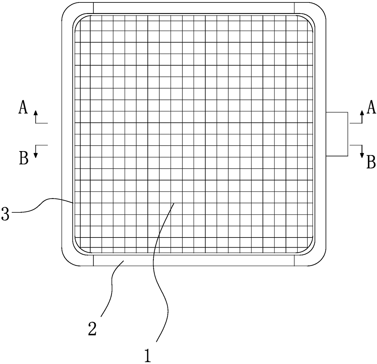
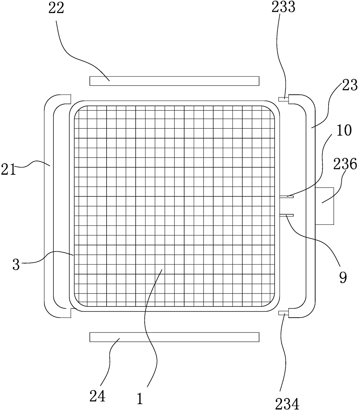
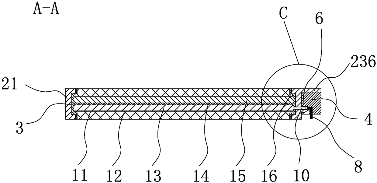
[0027] refer to Figure 1-Figure 4, the present embodiment is an anti-attenuation polysilicon wafer, comprising a silicon wafer main body 1, the silicon wafer main body 1 has a rectangular plate structure, and sequentially includes a tempered glass layer-11, a polyvinyl fluoride composite film 12, an N-type Silicon chip 13, conduction layer 14, P-type silicon chip 15 and tempered glass layer two 16, polyvinyl fluoride composite film 12 is fixed on the bottom surface of N-type silicon chip 13 by EVA sol, tempered glass layer one 11 is passed EVA sol Fixed on the bottom surface of polyvinyl fluoride composite film 12, toughened glass layer 2 16 is fixed on the top surface of P-type silicon chip 15 by EVA sol, the side of P-t...
PUM
 Abstract
Description
Claims
Application Information
 - R&D Engineer
- R&D Manager
- IP Professional
- Industry Leading Data Capabilities
- Powerful AI technology
- Patent DNA Extraction
Browse by: Latest US Patents, China's latest patents, Technical Efficacy Thesaurus, Application Domain, Technology Topic.
© 2024 PatSnap. All rights reserved.Legal|Privacy policy|Modern Slavery Act Transparency Statement|Sitemap