

A kind of epitaxy device of semiconductor light-emitting diode
A technology of light-emitting diodes and semiconductors, applied in semiconductor devices, electrical components, circuits, etc., can solve the problems of a large increase in the thickness of the epitaxial structure, a large increase in the growth cost, and an increase in the operating voltage of the device, so that the conductivity can be easily regulated and improved. Current spreading and small increase in device voltage
- Summary
- Abstract
- Description
- Claims
- Application Information
AI Technical Summary
Problems solved by technology
Method used
Image

Examples
Embodiment Construction
[0025] The present invention will be further described below in conjunction with the accompanying drawings and specific embodiments.
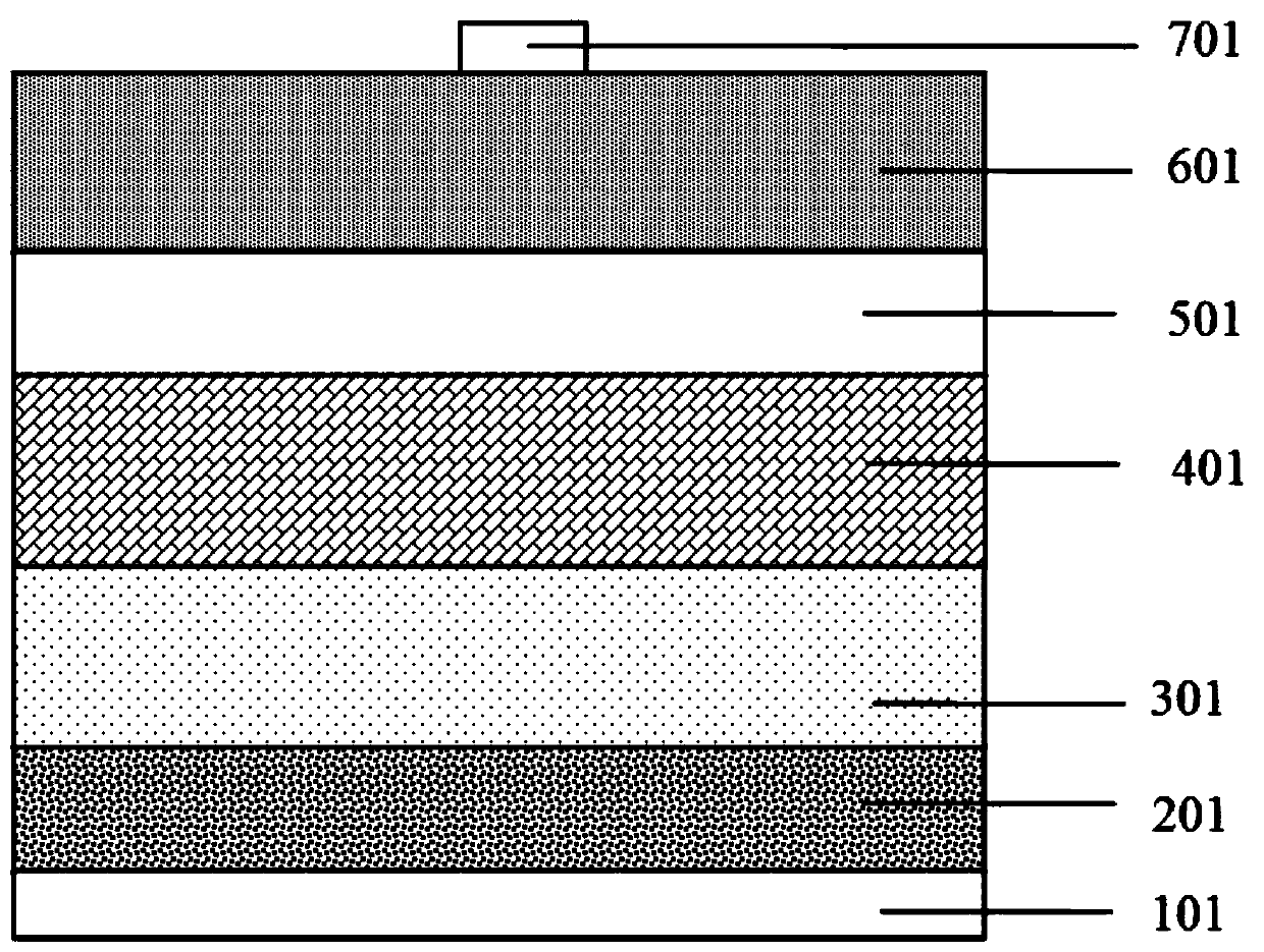
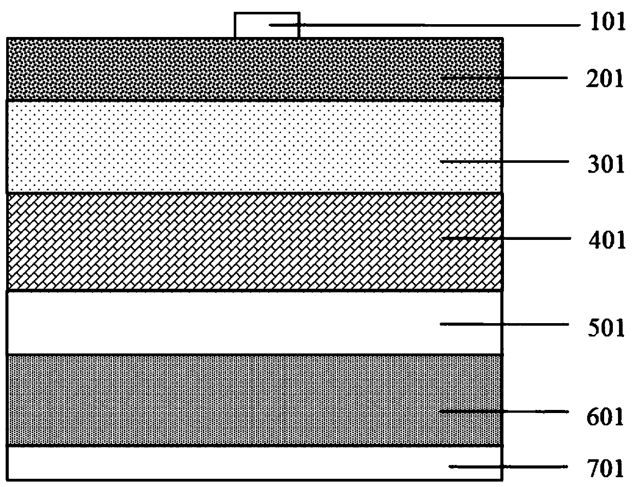
[0026] A kind of epitaxy device of semiconductor light-emitting diode of the present invention, as figure 1 As shown, it includes an N electrode 101, an N-type semiconductor contact layer 201 (in direct contact with the N electrode, used to adjust the contact resistance between the N electrode and the N-type semiconductor interface), an N-type semiconductor conductive layer 301, a light emitting layer 401, and a P-type semiconductor layer. Conductive semiconductor layer 501, P-type semiconductor contact layer 601 (in direct contact with the P electrode, used to adjust the contact resistance between the P electrode and the P-type semiconductor interface) and P electrode 701; between the N electrode 101 and the N-type semiconductor contact layer 201 The interface contact resistance is adjusted by the doping concentration of the N-type semiconduct...
PUM
 Abstract
Description
Claims
Application Information