

Active clamp voltage stress suppression circuit, method and drive circuit for power switch
A power switch and stress suppression technology, which is applied in the field of drive circuits and active clamp voltage stress suppression circuits, can solve the problems of current loss and affect the service life of active clamp effect TVS, so as to reduce heat loss and improve utilization rate, improve the effect of the clamping effect
- Summary
- Abstract
- Description
- Claims
- Application Information
AI Technical Summary
Problems solved by technology
Method used
Image

Examples
Embodiment 1
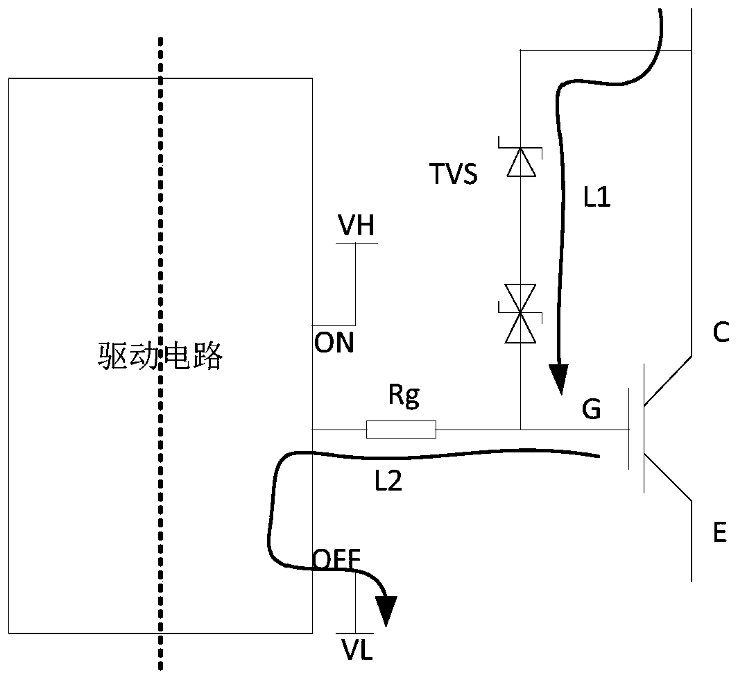
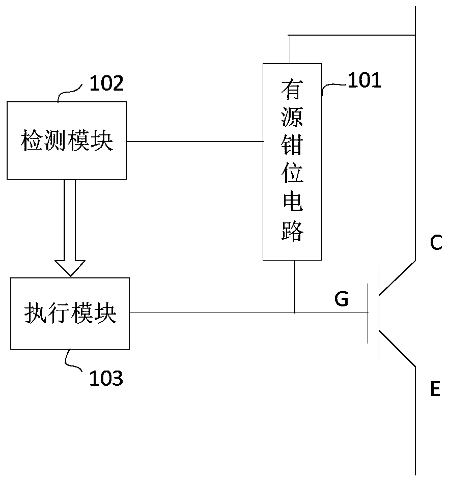
[0046] reference figure 1 An active clamp circuit 101 is connected between the input terminal and the control terminal of the power switch, and the power switch is not limited to IGBT, MOSFET, etc. For example, taking the IGBT as an example in this embodiment, the active clamping circuit 101 is connected between the collector and the gate of the IGBT. The active clamp voltage stress suppression circuit of the power switch of the present invention includes:
[0047] The detection module 102 is used to detect whether the power switch triggers an active clamp;
[0048] The execution module 103 is arranged in the drive path of the power switch, and is used to cut off the drive path when the detection module 102 detects that the active clamp is triggered.
[0049] It is understandable that when the active clamp is triggered, current will be injected into the power switch, so it is possible to determine whether the active clamp is triggered by detecting the magnitude of the current. In a...
Embodiment 2
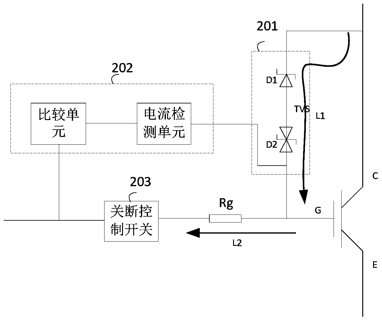
[0054] reference image 3 In this embodiment, the active clamp voltage stress suppression circuit of the power switch includes: a detection module 202 and an execution module 203. The detection module 202 includes a current detection unit and a comparison unit, and the execution module 203 includes a turn-off control switch, and the turn-off control switch is arranged in the current driving path of the power switch. The active clamp circuit 201 includes a unidirectional TVS tube D1 and a bidirectional TVS tube D2, and the power switch is an IGBT. Specifically:
[0055] The current detection unit is connected between the bidirectional TVS tube D2 in the active clamp circuit 201 and the gate G of the power switch, and is used to detect the output of the active clamp circuit 201 to the control terminal of the power switch That is, the current of the gate G, and the corresponding detection voltage is generated, and the current detection unit can be implemented by using a current samp...
Embodiment 3
[0061] reference Figure 4 , The power switch is an IGBT. In this embodiment, the suppression circuit includes: a detection module 302 and an execution module 303. The active clamping circuit 301 includes a unidirectional TVS tube D1, a bidirectional TVS tube D2, and a diode D3. The detection module 302 includes current sampling resistor R1, voltage divider resistors R2 and R3, comparator A1, analog-to-digital converter C1, and execution module 303 includes AND gate C2, digital-to-analog converter A3, turn-off control switch K2, and power switch drive The path includes a logic processing unit, a digital-to-analog converter A2, and a conduction control switch K1 that controls the conduction of the power switch.
[0062] Wherein, the first end of the bidirectional TVS tube D2 is connected to the anode of the diode D3, the cathode of the diode D3 is connected to the control end of the power switch, and the second end of the bidirectional TVS tube is connected to the anode of the un...
PUM
 Abstract
Description
Claims
Application Information