Array substrate line drive unit and circuit, and liquid crystal display panel

An array substrate row and drive unit technology, applied in the electronic field, can solve the problems of short effective charging time, insufficient rise time and fall time, and affect the charging efficiency of horizontal scanning lines, etc., to achieve long effective charging time, improve charging efficiency, Effect of reducing rise time and fall time

Inactive Publication Date: 2018-09-04
SHENZHEN CHINA STAR OPTOELECTRONICS SEMICON DISPLAY TECH CO LTD
View PDF6 Cites 24 Cited by
  • Summary
  • Abstract
  • Description
  • Claims
  • Application Information

AI Technical Summary

Problems solved by technology

[0004] The Gate signal actually output by the GOA circuit structure is one of the key factors determining the performance of the GOA. The Gate signal waveform can be divided into the low voltage stage, the first high voltage stage, and the second high voltage stage. In the above second high voltage stage, the Gate signal waveform The Rising Time (Rising Time) is the duration of rising to the second high voltage stage, and the Falling Time (FallingTime) is the duration of the second high voltage stage falling to the low voltage stage, because the rising time and falling time of the Gate signal waveform are not short enough , shortening the time to maintain the high level in the second high voltage stage will affect the charging efficiency on the horizontal scanning line, especially in the gate drive circuit using the tri-gate transistor (Tri-Gate) architecture, effective charging shorter time

Method used


Image

  • Array substrate line drive unit and circuit, and liquid crystal display panel
  • Array substrate line drive unit and circuit, and liquid crystal display panel
  • Array substrate line drive unit and circuit, and liquid crystal display panel

Examples


Embodiment Construction

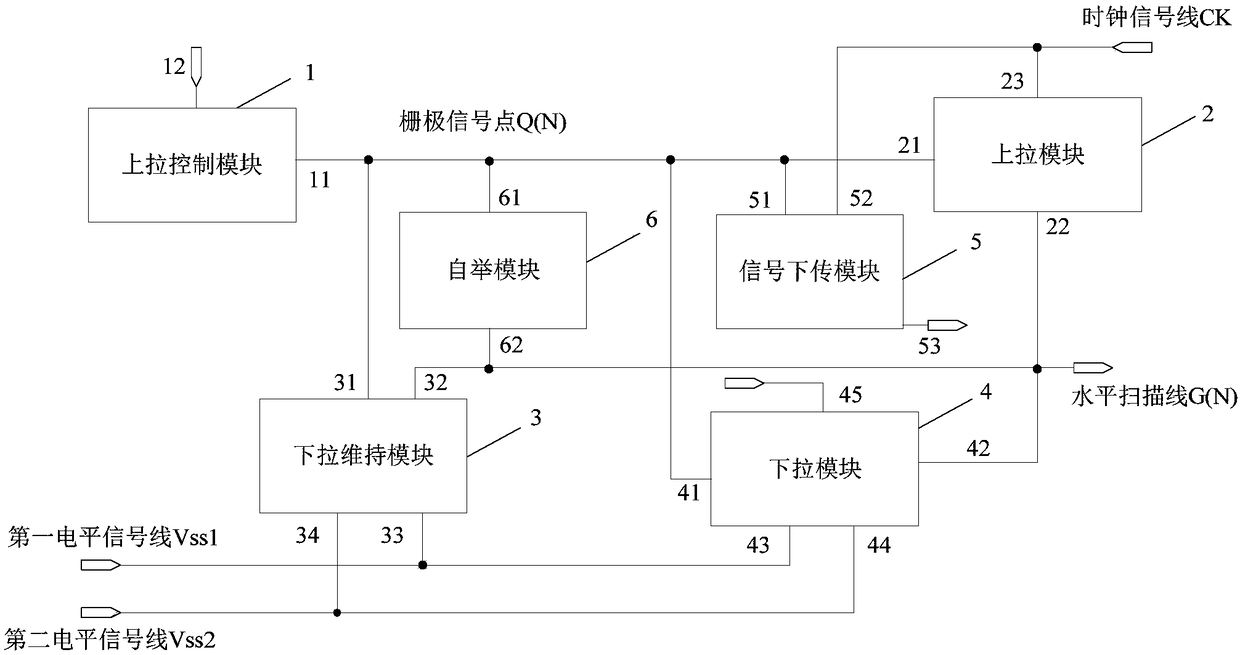
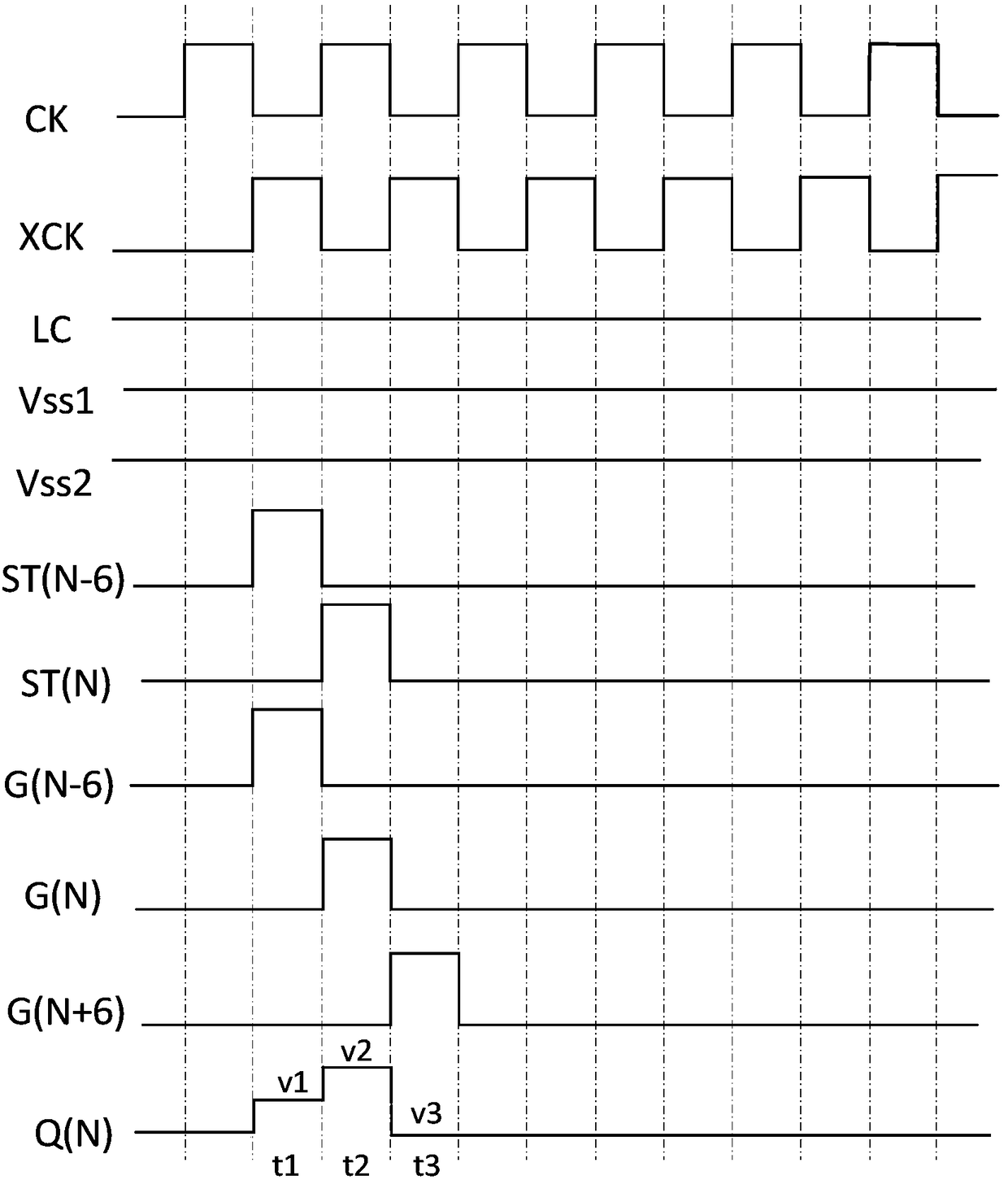
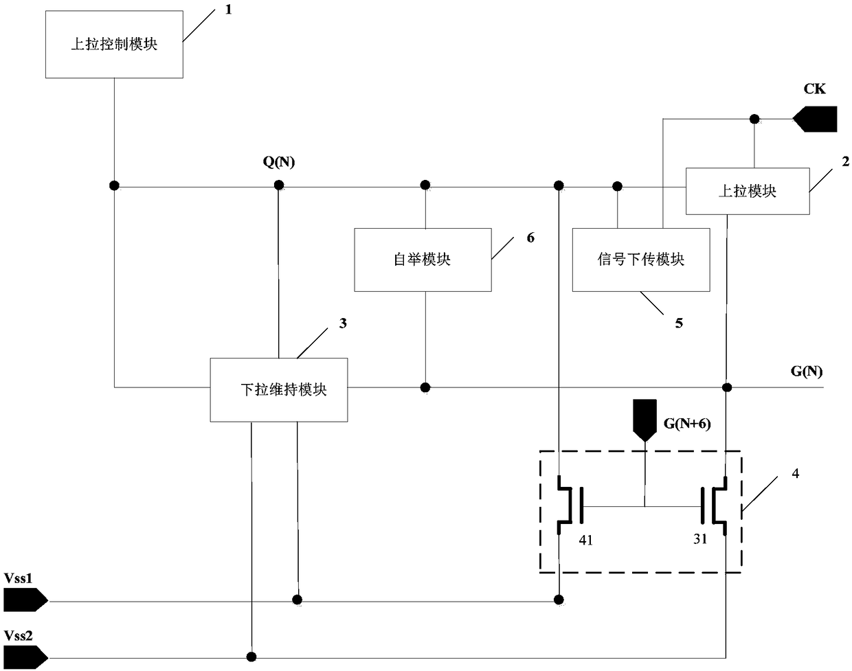
[0023] The following will clearly and completely describe the technical solutions in the embodiments of the present invention with reference to the accompanying drawings in the embodiments of the present invention. Obviously, the described embodiments are some of the embodiments of the present invention, but not all of them. Reference herein to an "embodiment" means that a particular feature, structure, or characteristic described in connection with the embodiment can be included in at least one embodiment of the present invention. The occurrences of this phrase in various places in the specification are not necessarily all referring to the same embodiment, nor are separate or alternative embodiments mutually exclusive of other embodiments. It is understood explicitly and implicitly by those skilled in the art that the embodiments described herein can be combined with other embodiments.

[0024] Based on the embodiments of the present invention, all other embodiments obtained ...


PUM


Abstract

The embodiment of the invention discloses an array substrate line drive unit and circuit, and a liquid crystal display panel. An output end of a pull-up control module of an array substrate line driveunit, a control end of a pull-up module, a first end of a pull-down maintenance module, a first end of a pull-up module, a control end of a signal download module and a first end of a bootstrap module are connected with a gate signal point, a second end of the pull-down maintenance module, a second end of the pull-down module, a second end of the bootstrap module and an output end of the pull-upmodule are connected with a horizontal scanning line, a third end of the pull-down maintenance module and a third end of the pull-down module are connected with a first level signal line, a fourth endof the pull-down maintenance module and a fourth end of the pull-down module are connected with a second level signal line, an input end of the pull-up module and an input end of the pull-down moduleare connected with a clock signal line; and the voltage of the first level signal line is smaller than the voltage of the second level signal line. The array substrate line drive unit and circuit, and a liquid crystal display panel can shorten the fall time of the gate signals and can improve the charge efficiency.

Description

technical field [0001] The invention relates to the field of electronic technology, in particular to an array substrate row driving unit, a circuit and a liquid crystal display panel. Background technique [0002] Array substrate row drive (Gate Driver On Array, GOA) technology is a kind of thin film transistor (ThinFilm Transistor, TFT) gate scanning drive circuit fabricated on the array substrate, to replace the driver chip made of external silicon chips technology. Since the GOA circuit can be directly fabricated around the panel, it can not only reduce the thickness of the frame of the panel of the Liquid Crystal Display (LCD), simplify the manufacturing process, but also reduce the product cost and improve the integration of the LCD panel. [0003] Existing GOA circuits usually include a plurality of cascaded GOA units, and each level of GOA unit includes a pull-up control circuit, a pull-up circuit, a downlink circuit, a pull-down circuit, a bootstrap capacitor, a pul...

Claims


Application Information

Patent Timeline
Patent Type & Authority Applications(China)
IPC IPC(8): G09G3/36G09G3/20
CPCG09G3/20G09G3/3677G09G2310/0286G09G3/3266
Inventor 陈仁禄曾勉
Owner SHENZHEN CHINA STAR OPTOELECTRONICS SEMICON DISPLAY TECH CO LTD
Why Eureka
Try Eureka