
14T radiation-resistant static storage cell

A static storage and anti-irradiation technology, applied in static memory, information storage, digital memory information, etc., can solve problems such as poor write margin, high power consumption, and slow circuit write speed, so as to reduce power consumption and improve resistance The ability of SEU and the effect of improving the writing speed

Active Publication Date: 2018-09-04
ANHUI UNIVERSITY
View PDF7 Cites 9 Cited by
  • Summary
  • Abstract
  • Description
  • Claims
  • Application Information

AI Technical Summary

Problems solved by technology

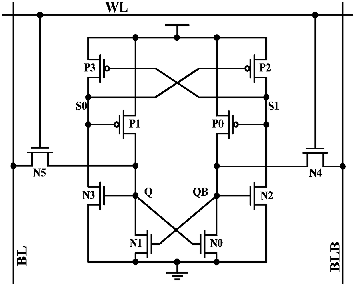
Compared with the traditional six-tube unit and Dual Interlocked Storage Cell (DICE) structure, it has better anti-SEU ability, but the unit has poor write margin and consumes a lot of power
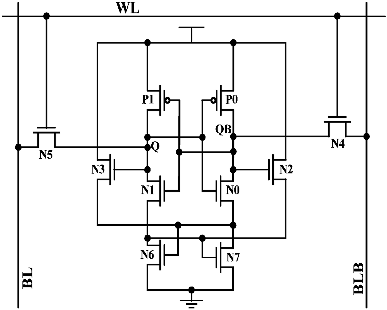
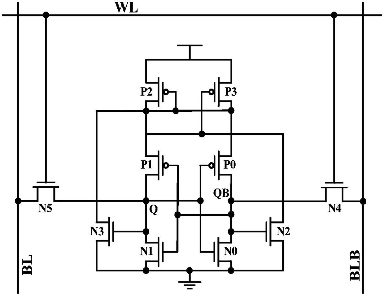
[0004] 2) if figure 2 and image 3 The two NovelSort Error Hardened 10T SRAM Cells circuits proposed by In-Seok Jung and Yong-Bin Kim in 2012 are hardened NMOS stacked 10T SRAM cell (NS10T) and hardened PMOS stacked 10T SRAM cell (PS10T). structure, in which the NS10T circuit can only restore the flip from 0 to 1, and the PS10T can only restore the flip from 1 to 0, and both circuits can solve the problem of multi-node disturbance caused by charge sharing, but the two circuits Slow write speed and high power consumption
But this circuit has slow write speed and poor read ability
[0006] 4) if Figure 5 Shown is a Highly ReliableMemory Cell (RHD12T) circuit proposed by Chunhua Qi and Liyi Xiao in 2016. This circuit greatly enhances the anti-SEU ability of the circuit by using source isolation technology. It can not only improve the anti-SEU ability of a single node but also It can improve the ability to resist multi-node flipping, but the writing speed of this circuit is slow and the power consumption is large

Method used


Image

  • 14T radiation-resistant static storage cell
  • 14T radiation-resistant static storage cell
  • 14T radiation-resistant static storage cell

Examples


Embodiment Construction

[0033] The technical solutions in the embodiments of the present invention will be clearly and completely described below in conjunction with the accompanying drawings in the embodiments of the present invention. Obviously, the described embodiments are only some of the embodiments of the present invention, not all of them. Based on the embodiments of the present invention, all other embodiments obtained by persons of ordinary skill in the art without making creative efforts belong to the protection scope of the present invention.

[0034] An embodiment of the present invention provides a 14T radiation-resistant static memory unit, such as Figure 6As shown, it mainly includes: six NMOS transistors and eight PMOS transistors; the six NMOS transistors are sequentially marked as N0~N5, and the eight PMOS transistors are sequentially marked as P0~P7; the PMOS transistor P1 and the NMOS transistor N1 form an inverting PMOS transistor P0 and NMOS transistor N0 form another inverter...


PUM


Abstract

The invention discloses a 14T radiation-resistant static storage cell, which is capable of improving SEU (Single Event Upset) resistance, improving the speed of the 14T radiation-resistant static storage cell to a large extent under the situation that smaller cell area is sacrificed and reducing power consumption. During a reading-writing stage, a WL signal is in high level. When a circuit is in awriting stage, if BL is in high level and BLB is in low level, '1' can be written in a storage node Q through differential input transistors N4 and N5; if the BL is in low level and the BLB is in high level, '0' can be written in the storage node Q through the differential input transistors N4 and N5. When the circuit is in a reading stage, if the BL and the BLB are both in high level and data stored in the cell unit is '1' voltage can be discharged to the ground through transistors N4 and N0 by the BLB, voltage difference can be generated by a bit line, and then the data can be read out through a sensitive amplifier; if the data stored in the cell circuit is '0', the current can be discharged to the ground through transistors N5 and N1 by the BL, the voltage difference can be generated by the bit line, and then the data can be read out through the sensitive amplifier.

Description

technical field [0001] The invention relates to the field of integrated circuit design, in particular to a unit circuit structure capable of increasing the writing speed of a storage unit, reducing unit power consumption and improving the ability of the unit to resist Single Event Upset (abbreviated as SEU). It is a 14T Radiation-resistant static storage unit. Background technique [0002] With the reduction of feature size and power supply voltage, the circuit is more and more sensitive to radiation, and the single event effect (Single Event Effect, abbreviated as SEE) becomes an inevitable problem, which makes the development of SEE radiation resistance hardening technology in combinational circuits very urgent. . SEU is a form of SEE, which is a soft error and non-destructive. When heavy ion particles are incident on the semiconductor material, the excess charges will be ionized, and these excess charges will be collected by the electrodes of the device, resulting in er...

Claims


Application Information

Patent Timeline
IPC IPC(8): G11C11/412
CPCG11C11/4125
Inventor 彭春雨黄家提孔令雨肖松松吴秀龙蔺智挺高珊陈军宁
Owner ANHUI UNIVERSITY
Learn More