Thin film encapsulation structure, display device and preparation method of display device

A thin-film packaging and display device technology, which is applied in semiconductor/solid-state device manufacturing, electrical components, electrical solid-state devices, etc., can solve the problems of short distance between display layers, affecting touch effects, and signal interference on touch layers, so as to improve and prevent , The effect of improving the mechanical properties of the film and improving the electromagnetic shielding performance

Pending Publication Date: 2018-09-04
YUNGU GUAN TECH CO LTD
View PDF11 Cites 13 Cited by
  • Summary
  • Abstract
  • Description
  • Claims
  • Application Information

AI Technical Summary

Problems solved by technology

[0005] However, due to the thin packaging film layer (usually about 10 μm), the distance between the touch layer and the OLED display layer is very close, and the cathode of the OLED will cause signal interference to the touch layer, thus affecting the touch effect

Method used


Image

  • Thin film encapsulation structure, display device and preparation method of display device
  • Thin film encapsulation structure, display device and preparation method of display device

Examples


Embodiment 1

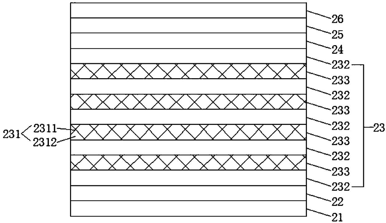
[0040] This embodiment provides a display device, such as figure 2 As shown, it includes a substrate 21, an OLED display layer 22, a film packaging structure 23, a touch layer 24, a polarizer 25 and a cover plate 26.

[0041] The substrate 21 includes a base substrate, a thin film transistor (TFT) array layer provided on the base substrate, and a flat layer on the array layer. The base substrate may be formed of various materials such as glass, plastic, silicon or metal, and preferably, glass is used as the base substrate.

[0042] The OLED display layer 22 is disposed on the substrate 21, and the layer includes organic electroluminescence units (OLED) with R, G, and B three-color pixel arrays. The organic electroluminescence unit has a first electrode, a second electrode, and a first electrode. The organic functional layer between the electrode and the second electrode. Among them, the first electrode is an anode, such as ITO material; the second electrode is a cathode, such as...

Embodiment 2

[0049] This embodiment provides a method for manufacturing the display device as in Embodiment 1, including:

[0050] (1) Provide a substrate 21, and form an OLED display layer 22 on the substrate 21;

[0051] Specifically, a thin film transistor (TFT) array layer is formed on a glass substrate, and a flat layer is formed on the thin film transistor (TFT) array layer; a transparent ITO conductive film is vapor-deposited on the flat layer to obtain an anode; and then the anode is vapor-deposited Hole injection layer, hole transport layer, light emitting layer, electron transport layer, electron injection layer and cathode Mg / Ag to obtain an OLED display layer.

[0052] (2) In step (1), an inorganic material passivation layer 232 and an organic material buffer layer 233 are alternately formed on the OLED display layer 22 in order, wherein an electromagnetic shielding layer 231 is provided in at least one organic material buffer layer 233, Forming a packaging film structure 23;

[0053]...

Embodiment 3

[0057] The present invention provides a display device. The difference from Embodiment 1 is that the thin film encapsulation layer 23 is not provided between the OLED display layer 22 and the touch layer 24, and only the electromagnetic shielding layer 231 is provided. In the display device of this structure, the electromagnetic shielding layer 231 can still shield the interference of the cathode of the OLED display layer 22 to the signal of the touch control layer 24.


PUM


Abstract

The present invention belongs to the display technological field and relates to a thin film encapsulation structure, a display device, and a preparation method of the display device. The thin film encapsulation structure provided by the invention comprises a thin film encapsulation layer and electromagnetic shielding layers; the electromagnetic shielding layers are located in the thin film encapsulation layer; each electromagnetic shielding layer comprises a wire mesh formed by metal material; and the electromagnetic shielding layers isolate two side surface regions of the thin film encapsulation structure from each other, so that the thin film encapsulation structure has an electromagnetic interference shielding function; inorganic material passivation layers and organic material buffer layers are alternately arranged in the thin film encapsulation layer, and therefore, the thin film encapsulation structure has an excellent water and oxygen barrier property, the encapsulation effect of the thin film encapsulation structure can be improved, the aging of organic materials can be prevented, and the service life of an OLED device can be prolonged. The invention also provides a displaydevice comprising electromagnetic shielding layers; and the electromagnetic shielding layers isolate an OLED display layer from a touch control layer, and shield signals generated by the cathode of the OLED display layer, and therefore, the interference of the signals generated by the cathode on the signals of the touch control layer can be weakened or eliminated, and touch control performance can be improved.

Description

Technical field [0001] The invention belongs to the field of display technology, and specifically relates to a thin film packaging structure, a display device and a preparation method of the display device. Background technique [0002] Organic Light-Emitting Diode (OLED) has self-luminescence, low driving voltage, high luminous efficiency, short response time, high definition and contrast, close to 180° viewing angle, wide operating temperature range, and can achieve flexible display and large Area full-color display and many other advantages are recognized by the industry as the display device with the most development potential. The principle of light emission is to use ITO glass transparent electrode and metal electrode as the anode and cathode of the device respectively. Under a certain voltage drive, electrons and holes are injected from the cathode and anode to the electron transport layer and hole transport layer respectively, and then migrate respectively. In the light-...

Claims


Application Information

Patent Timeline
Patent Type & Authority Applications(China)
IPC IPC(8): H01L51/52H01L27/32
CPCH10K59/40H10K50/8445H10K59/1201
Inventor 程芸
Owner YUNGU GUAN TECH CO LTD
Why Eureka
Try Eureka