Terahertz antenna structure and radiation source and detector comprising same

An antenna structure and terahertz technology, applied in the terahertz field, can solve the problems of low matching efficiency between terahertz antennas and photoconductors, reduce antenna input resistance, etc., and achieve the effects of improving detection sensitivity, increasing input resistance, and small absorption coefficient

Active Publication Date: 2018-09-04
FUJIAN INST OF RES ON THE STRUCTURE OF MATTER CHINESE ACAD OF SCI
View PDF5 Cites 1 Cited by
  • Summary
  • Abstract
  • Description
  • Claims
  • Application Information

AI Technical Summary

Problems solved by technology

Although the double-layer substrate composed of thicker low-temperature gallium arsenide and high-resistance silicon can couple the terahertz wave into the free space and improve the directivity, the effective dielectric constant of the double-layer substrate is higher than 11.9 above, greatly reducing the antenna input resistance
Although the directivity is improved, it cannot solve the problem of low matching efficiency between the terahertz antenna and the photoconductor

Method used


Image

  • Terahertz antenna structure and radiation source and detector comprising same
  • Terahertz antenna structure and radiation source and detector comprising same
  • Terahertz antenna structure and radiation source and detector comprising same

Examples


Embodiment 1

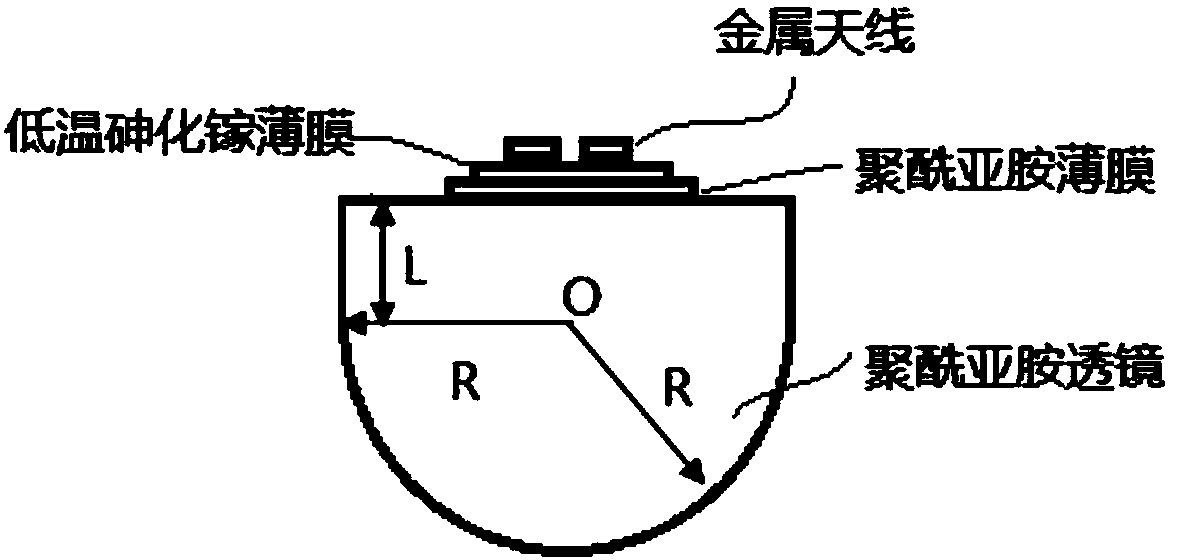
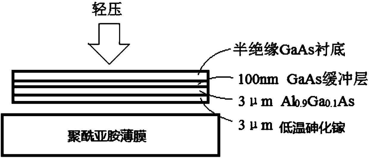
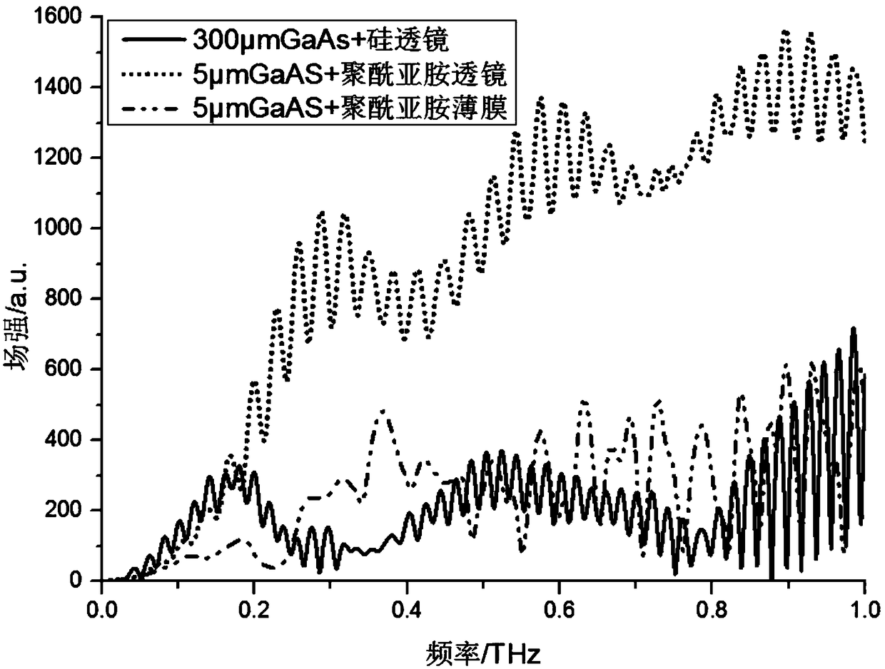
[0029] The traditional terahertz antenna processing method is to evaporate a metal antenna on a semiconductor substrate with a thickness of 300 microns, and then directly paste a silicon lens on the back. Because the semiconductor substrate of the structure of the present invention is only several microns thick, the traditional substrate thinning process is no longer applicable, and needs to be prepared by the following method: first, by epitaxial layer transfer technology, the semiconductor substrate film is transferred from The sacrificial layer is peeled off and transferred to a substrate of low dielectric constant material. Then the metal antenna is evaporated on the semiconductor substrate film. Finally, a lens made of low dielectric constant material is pasted on the back. The specific structure is as figure 1 with figure 2 shown. Specifically as follows:

[0030] A 100nm-thick GaAs buffer layer was grown on a (100)-oriented semi-insulating GaAs substrate by molecu...


PUM


Abstract

The invention belongs to the technical field of terahertz, and particularly relates to a terahertz antenna structure and a radiation source and detector comprising the same. The thickness of a semiconductor substrate of a conventional terahertz antenna structure is reduced to several micrometers from hundreds of micrometers, a high-dielectric constant silicon lens is substituted by a low-dielectric constant lens, thus, the input resistance of a metal antenna is improved, and the matching efficiency and the directivity are improved. By the terahertz antenna structure, the output power can be effectively improved by two or three times, and the detection sensitivity can be effectively improved; when the antenna is used as the radiation source, the output power is improved; and when the antenna is used as the detector, the detection sensitivity is improved.

Description

technical field [0001] The invention belongs to the technical field of terahertz, and in particular relates to a terahertz antenna structure and a radiation source and a detector including the antenna structure. Background technique [0002] Terahertz radiation is an electromagnetic wave with a frequency between 0.1THz and 10THz, which has great application prospects in security inspection, medical treatment, communication and other fields. For a long time, the development of terahertz sources (radiation sources) with high radiation intensity has been one of the key technologies of terahertz technology. Among them, the photoconductive antenna technology based on semiconductor materials has the advantages of working at room temperature, portability, and low price. However, due to the high resistivity of semiconductor materials, the resistance of the photoconductor in the illuminated gap area of ​​the antenna is generally above 10,000 ohms, while the input resistance of the p...

Claims


Application Information

Patent Timeline
Patent Type & Authority Applications(China)
IPC IPC(8): H01Q1/22H01Q1/38H01Q15/08H01Q19/06G01J1/42
CPCH01Q1/225H01Q1/38H01Q15/08H01Q19/06G01J1/42Y02P70/50
Inventor 陈景源林中晞林琦徐玉兰苏辉钟杏丽朱振国薛正群
Owner FUJIAN INST OF RES ON THE STRUCTURE OF MATTER CHINESE ACAD OF SCI
Why Eureka
Try Eureka